Programming_mail.pdf - 第13页
I- 5 Programming Manual Part I Basic Operation <<Enlarged View Screen>> 㹂 㹂 㹂 㹂 Press “D” Press “D” Press “D” Press “D” (a) SideLight Image (b) LowLight Image (c) T opLight (Coaxial Overhead Light) Image (d) …
I-4
Programming Manual
Part I Basic Operation
1.1.4 Changing the Magnifi cation
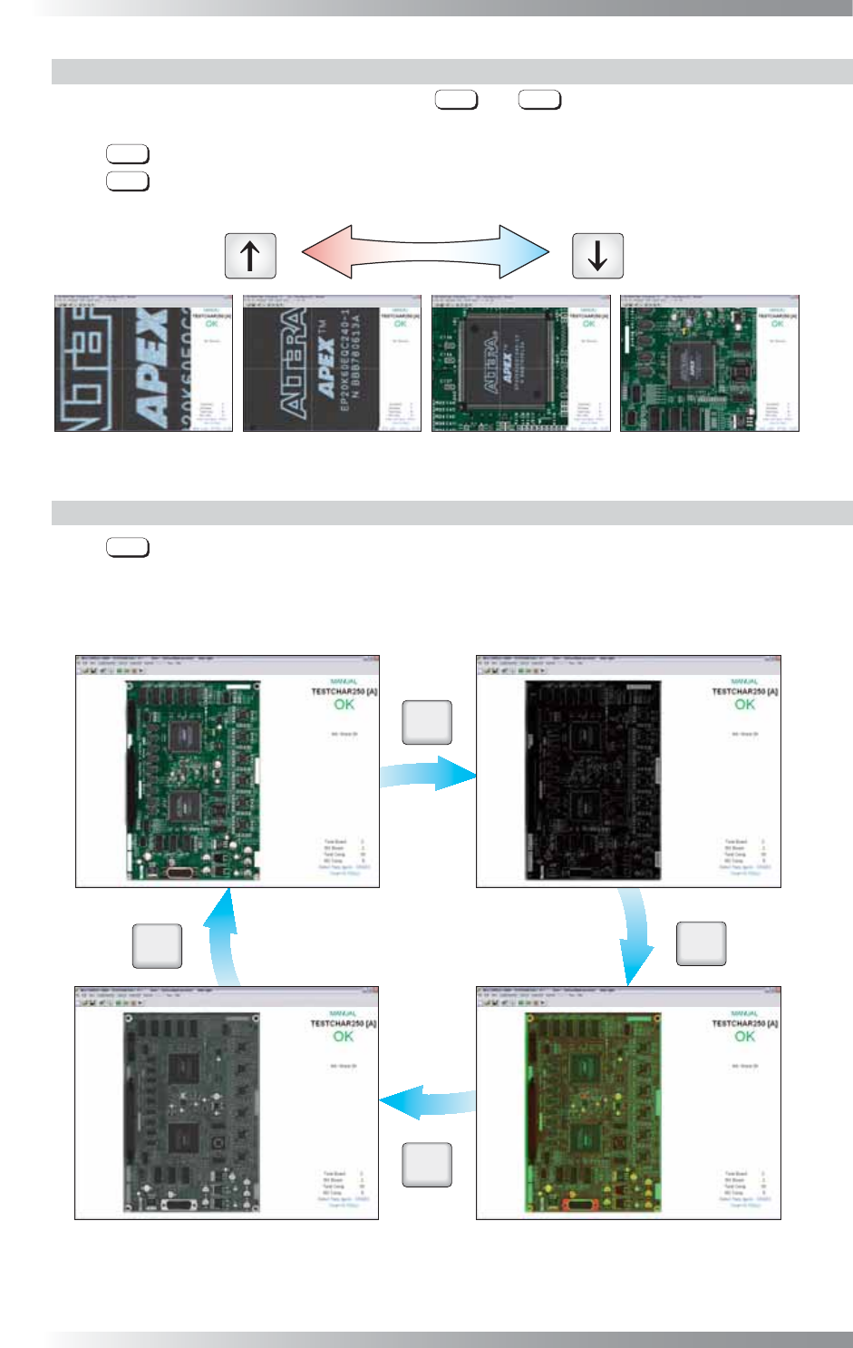
The magnifi cation can be changed by pressing
↑
and
↓
in Enlarged View Screen.
The same operation is available by scrolling wheel of mouse.
Press
↑
or scroll wheel of mouse upward to zoom in the image.
Press
↓
or scroll wheel of mouse downward to zoom out the image.
Magnification
Up Down
3UHVV³Ĺ´ 3UHVV³Ļ´
Figure 1-5 Changing the Magnifi cation
1.1.5 Switching Between the Images
Press
D
to switch images among TopLight (Coaxial Overhead Light), SideLight, and LowLight.
<<Full View Screen>>
Press “D”
Press “D”
Press “D”
Press “D”
(a) SideLight Image
(b) LowLight Image
(c) TopLight (Coaxial Overhead Light) Image
(d) Multi-Lighting Image
㹂
㹂
㹂
㹂
Figure 1-6 Switching Images in the Full View Screen
I-5
Programming Manual
Part I Basic Operation
<<Enlarged View Screen>>
㹂
㹂
㹂
㹂
Press “D”
Press “D”
Press “D”
Press “D”
(a) SideLight Image (b) LowLight Image
(c) TopLight (Coaxial Overhead Light) Image (d) Multi-Lighting Image
Figure 1-7 Switching Images in the Enlarged View Screen
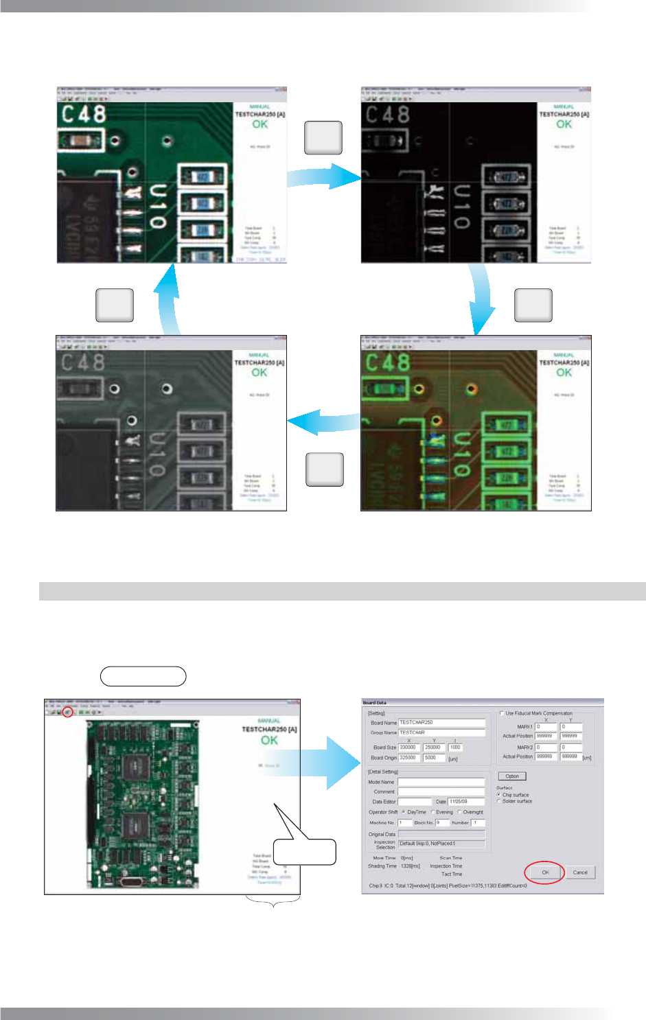
1.1.6 Board Setting
Open the Board Data dialog shown in Figure 1-8 to verify the PCB size, set or edit the PCB data.
Press the Board Setting button on the tool-bar or right-click the index frame to open the dialog.
After all the settings are completed, press OK.
NOTE
The above operation is available in Full View Screen and Enlarged View Screen.
Right-click
Index Frame
Figure 1-8 Board Data Edit
I-6
Programming Manual
Part I Basic Operation
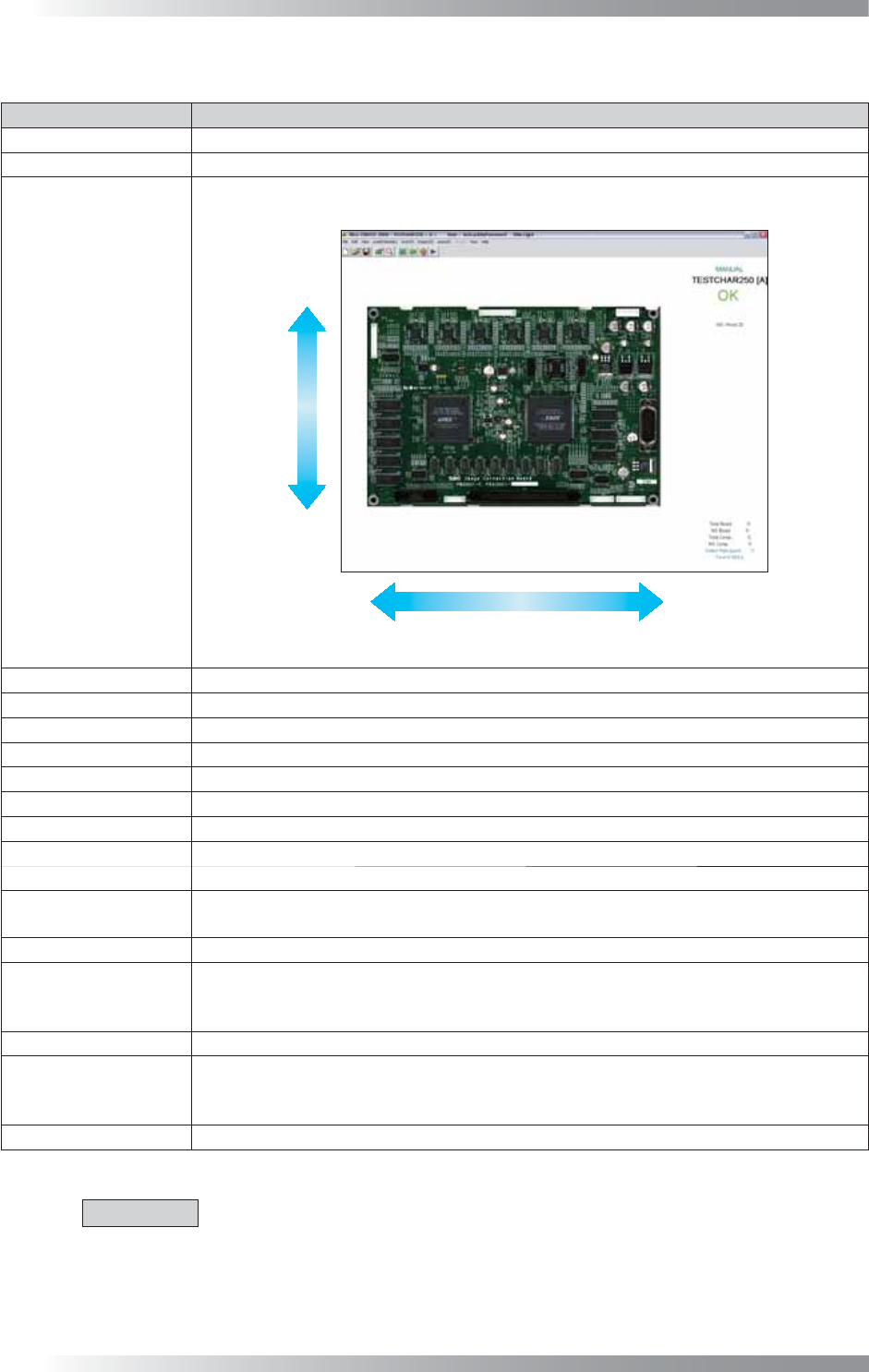
The table below describes the items in Board Data Edit dialog.
Item Description
Board Name
Displays the target PCB name.
Group Name
Displays the group name which has the same library with the target PCB.
Board size
Sets the target PCB size (μm). X-axis and Y-axis are set as shown below.
t indicates PCB thickness. (*1)
Y
X
Figure 1-9 Board Size Setting
Board Origin
Sets the PCB origin.
Model Name Not available.
Comment
Enter any comments if necessary.
Data Editor
Enter data creator.
Date
Created date (Month/Day/Year).
Operator Shift
Work shift.
Block No. Enter the number of sub-PCBs, if necessary.
Machine No. Not available.
Number Not available.
Use Fiducial Mark
Compensation
Enables fi ducial marks to correct misalignment.
MARK1
Sets the position of the fi rst fi ducial mark in X and Y coordinates.
Actual Position
Displays the actual position of a fi ducial mark in X and Y coordinates. The gap against the
MARK1 value represents the amount of deviation between the inspection data and
scanned image.
MARK2
Sets the position of the second fi ducial mark in X and Y coordinates.
Actual Position
Displays the actual position of a fi ducial mark in X and Y coordinates. The gap against the
MARK2 value represents the amount of deviation between the inspection data and
scanned image.
Option Not available.
Table 1-1 Each Item of
Board Data Edit
CAUTION
(*1) In case of BF-Comet10, BF-Comet18, and BF-Sirius, longitudinal direction is X and
lateral direction is Y.