SM482PLUS_Admin(Eng_Ver2.8).pdf - 第132页
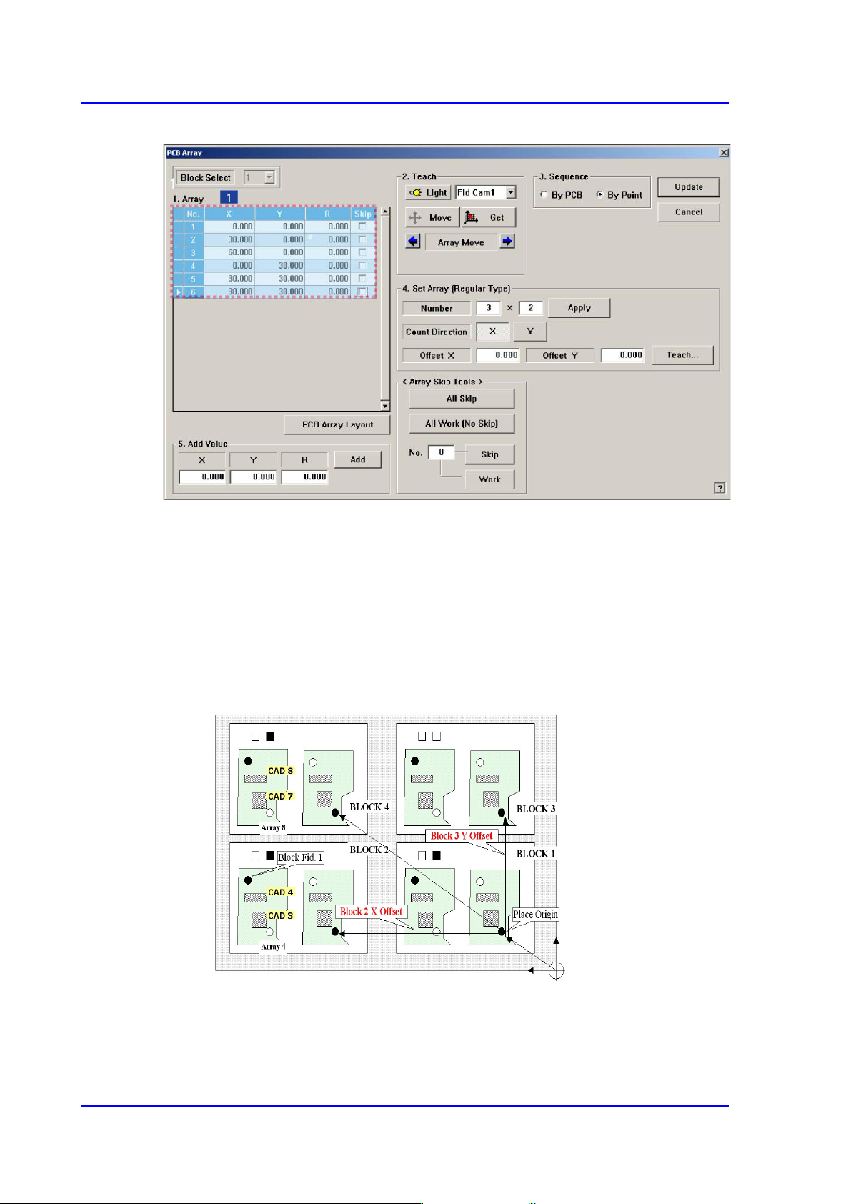
6-14 Multi-Functional Placer SM482( L) PLUS Administrator’s Guide Figure6.3 “PC B Array” dialog box 1: Gr id Cell <Block Select> combo box For a Multi PCB The model selected from the “Board De finition” dialog …
6-13
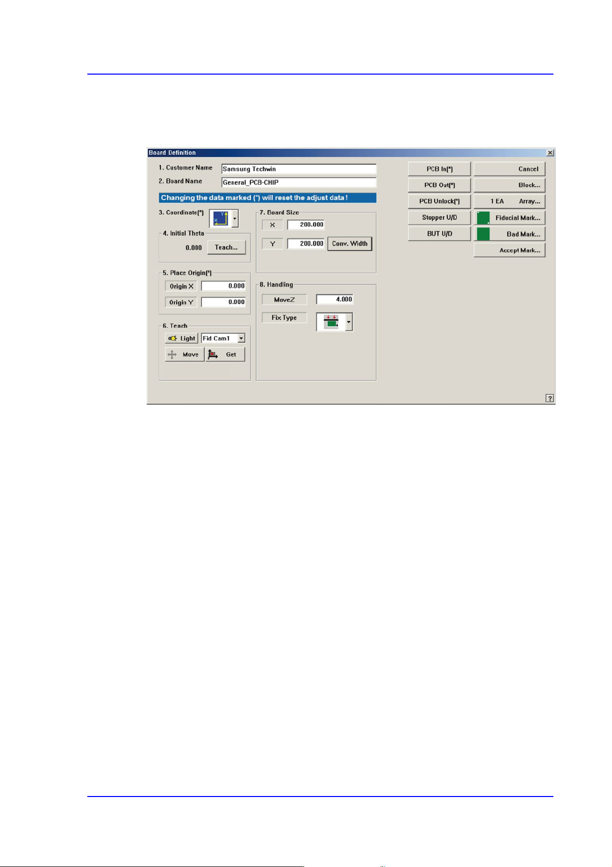
Board Definition
6.2. Array PCB Setup
For an array PCB, setup the offset value between the origin of the small PCB in the array
PCB and place origin of the array PCB.
When this <Array…> button is clicked on, the following dialog box is displayed.
6-14
Multi-Functional Placer SM482(L) PLUS Administrator’s Guide
Figure6.3 “PCB Array” dialog box
1: Grid Cell
<Block Select> combo box
For a Multi PCB
The model selected from the “Board Definition” dialog box is selected
automatically and the corresponding Combo Box is disabled.
For a Block PCB
Select the model for which setup will be performed and set other items.
<1. Array> group
Set the offset value of Array PCB from the “Place Origin” of the PCB. Lines
corresponding to the number of small PCBs in the array PCB setup in <4. Set Array
(Regular Type)> are made.
6-15
Board Definition
<No.> column
Set the offset value of Array PCB from the “Place Origin” of the PCB. Lines
corresponding to the number of small PCBs in the array PCB setup in <4. Set
Array (Regular Type)> are made.
<Skip.> column
Used to select the small PCB that will not be worked on among those in the Array
PCB. The machine continues to work without working on the small PCB selected
here.
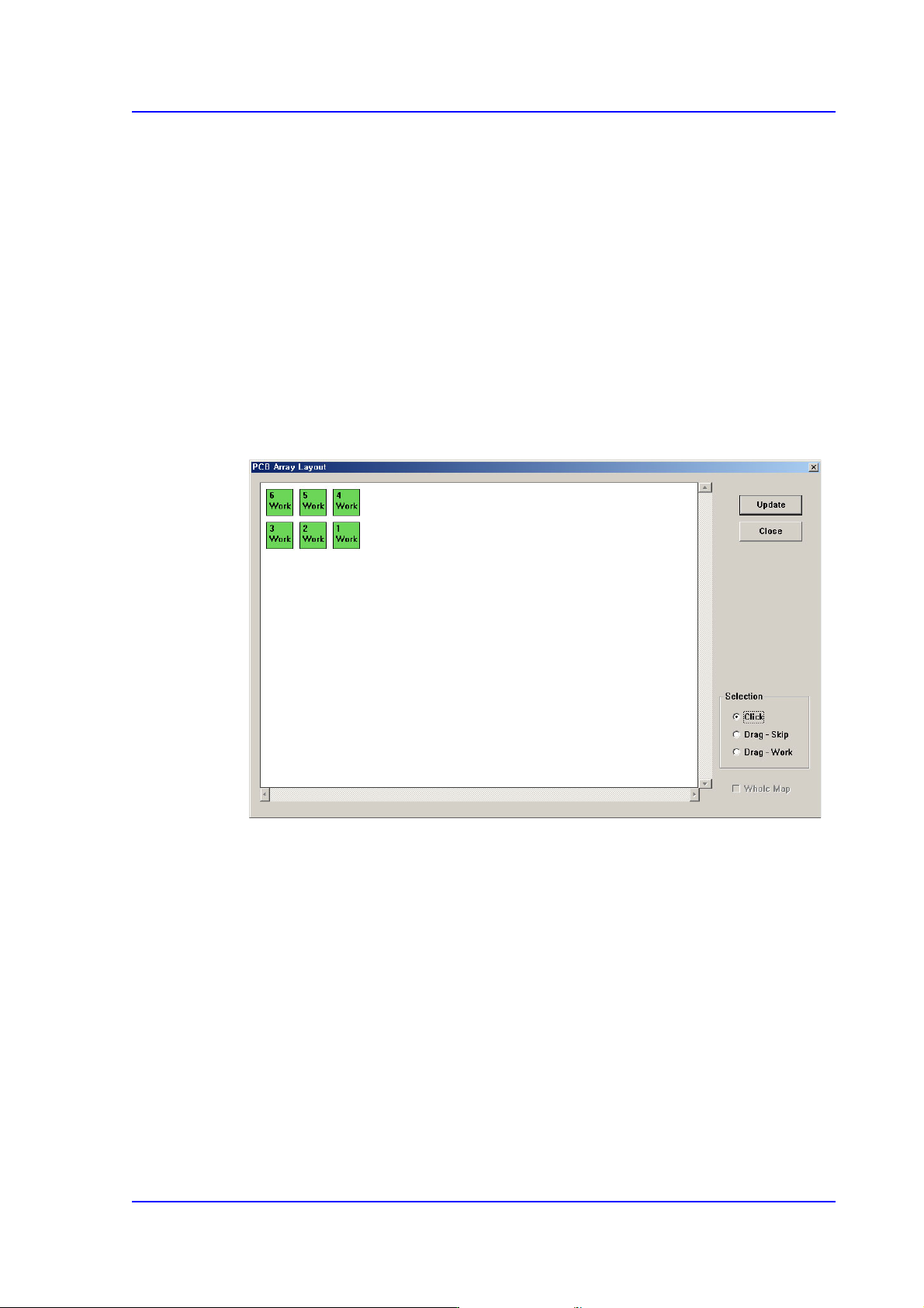
<PCB Array Layout> button
Used to determine whether to work on the corresponding PCB while watching the
arrangement of small PCBs in the Array PCB when selecting the small PCB that will
not be worked on among small PCBs in the Array PCB.
<Selection> option box group
[‘Work’ –Work on the PCB; ‘Skip’ –Not to work on the PCB]
<Click> option box
If the small PCB displayed on the ‘PCB Array Layout’ dialog box is selected
using the mouse with this option box selected, the setup of the corresponding
small PCB is changed.
If the small PCB set to ‘Work’ is selected, ‘Work’ is changed to ‘Skip’. If the
small PCB set to ‘Skip’ is selected, ‘Skip’ is changed to ‘Work’.
<Drag-Skip> option box
After this option box is selected if the small PCBs displayed on the ‘PCB
Array Layout’ dialog box are selected by dragging the mouse, the setup of the
selected small PCBs is changed to ‘Skip’. It is useful when selecting several
small PCBs at once.