SM482PLUS_Admin(Eng_Ver2.8).pdf - 第149页
6-31 Board Definition 6.3.1. Fiducial Mark Setup Order 1) Block Setup Omitted for non-block PC 2) Position T ype’ setup 3) Mark Position’ setup Select a fiducial mark in the <Mark Position> group. Click the <Mov…
6-30
Multi-Functional Placer SM482(L) PLUS Administrator’s Guide
applied, or in the image (Binary) to which threshold is applied as recognized by MMI.
<Test> button
By using the registered mark information, tests the fiducial mark.. The accuracy of the
registered mark data can be verified. When the test is successful, the following
message box is displayed.
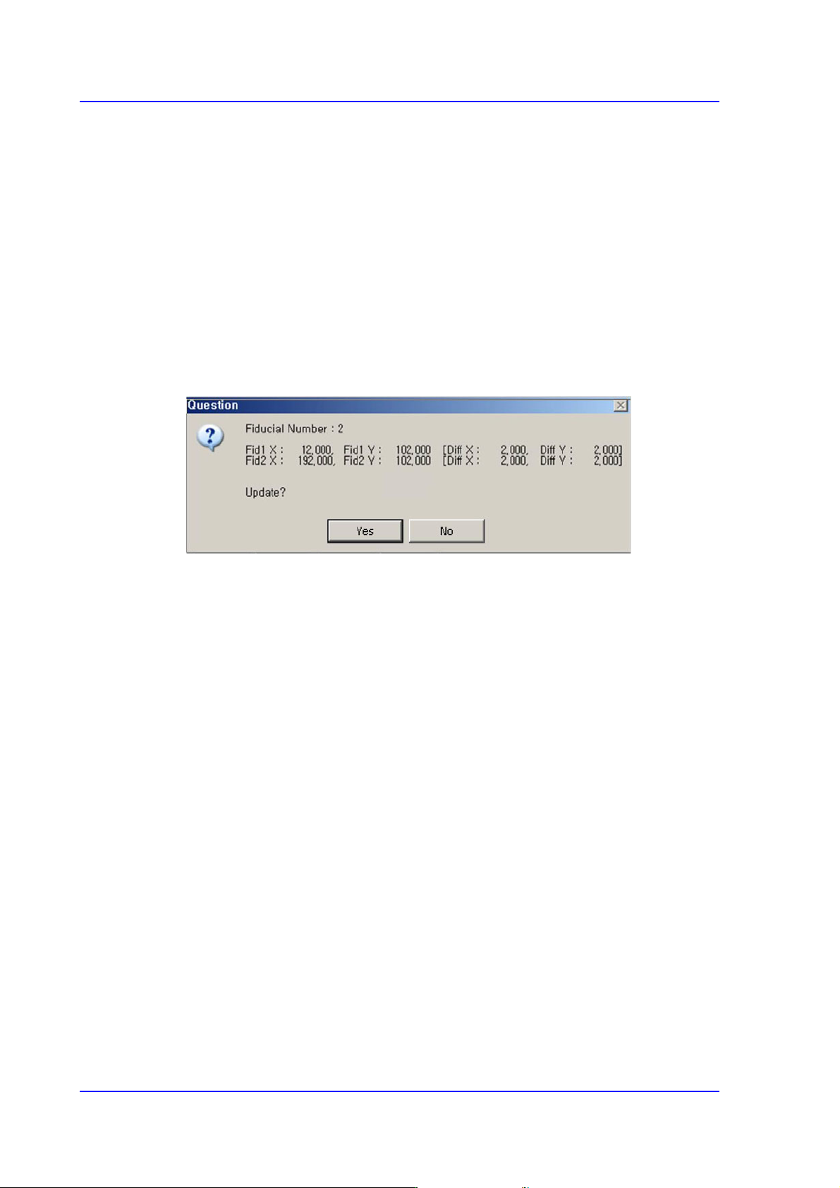
<Scan> button
Executes a scan test on the set fiducial mark. Mark recognition is performed to
minimize the teaching offset for the center points (2 points) of the fiducial mark.
Move the fiducial camera to the position of the set coordinate and recognize the mark.
After recognition of the mark, the offset is indicated as shown in the following figure.
When it is desired to compensate the offset, select “Yes”.
When placing the IC part whose lead pitch is 0.5, use this function to perform
compensation for the fiducial mark.
<OK> button
Saves the fiducial mark data and closes the <Fiducial Position & Mark> dialog box.
<Cancel> button
Closes the <Fiducial Position & Mark> dialog box without saving the fiducial mark
data.
6-31
Board Definition
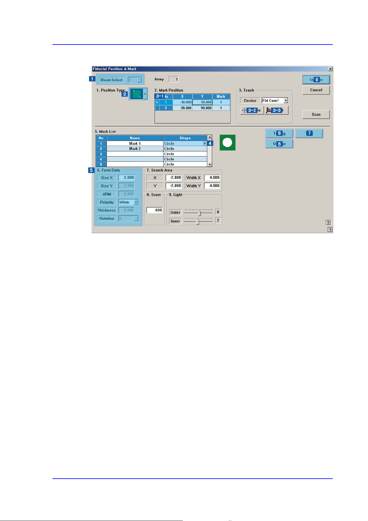
6.3.1. Fiducial Mark Setup Order
1) Block Setup
Omitted for non-block PC
2) Position Type’ setup
3) Mark Position’ setup
Select a fiducial mark in the <Mark Position> group.
Click the <Move> button to move the fiducial camera to the selected fiducial mark.
Perform adjustments so that the center of the fiducial mark falls on the crosshair center
of the SMVision window.
Click the <Get> button to input the coordinate of the fiducial mark.
4) ‘Mark List’ setup
5) ‘Form Data’ setup
6) Outline check
Click the <Outline> button to check if the outline seen in the SMVision window falls
on the fiducial mark outline.
If not, revise the “Shape Information’.
7) Fiducial mark recognition test
8) Tuning
Perform tuning at least more than twice.
9) Reflect set value: Click the <Update> button
6-32
Multi-Functional Placer SM482(L) PLUS Administrator’s Guide
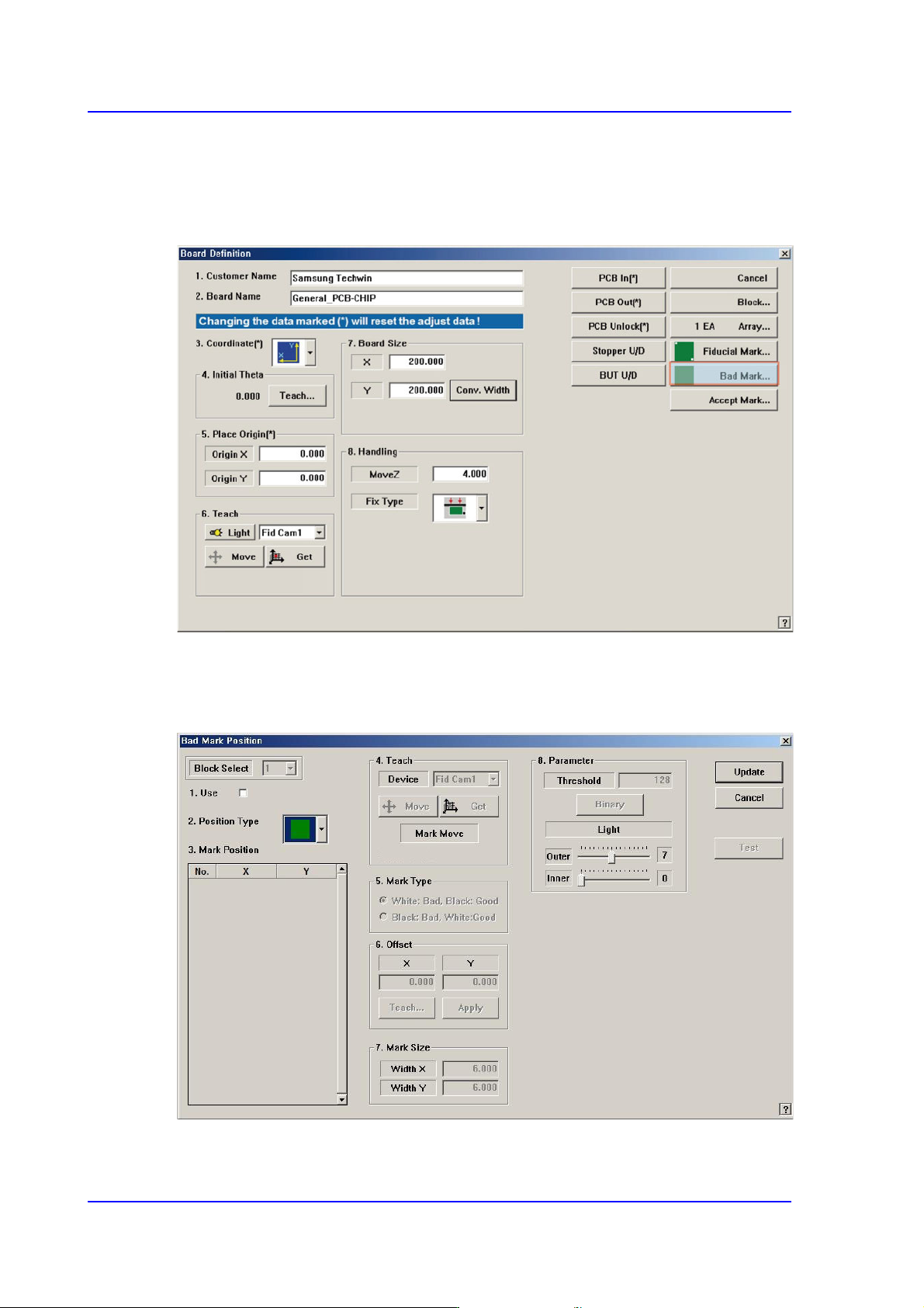
6.4. Bad Mark Setup
The ‘Bad Mark’ refers to the mark indicated on the PCB to show whether a small PCB in
the array PCB is good or defective. Placement is not performed on the small PCB
indicated defective.
When this <Bad Mark…> button is clicked on, the following dialog box to edit bad mark
data is displayed.
Figure6.6 “Bad Mark Position” dialog box (When the Position Type is “None”)