SM482PLUS_Admin(Eng_Ver2.8).pdf - 第150页
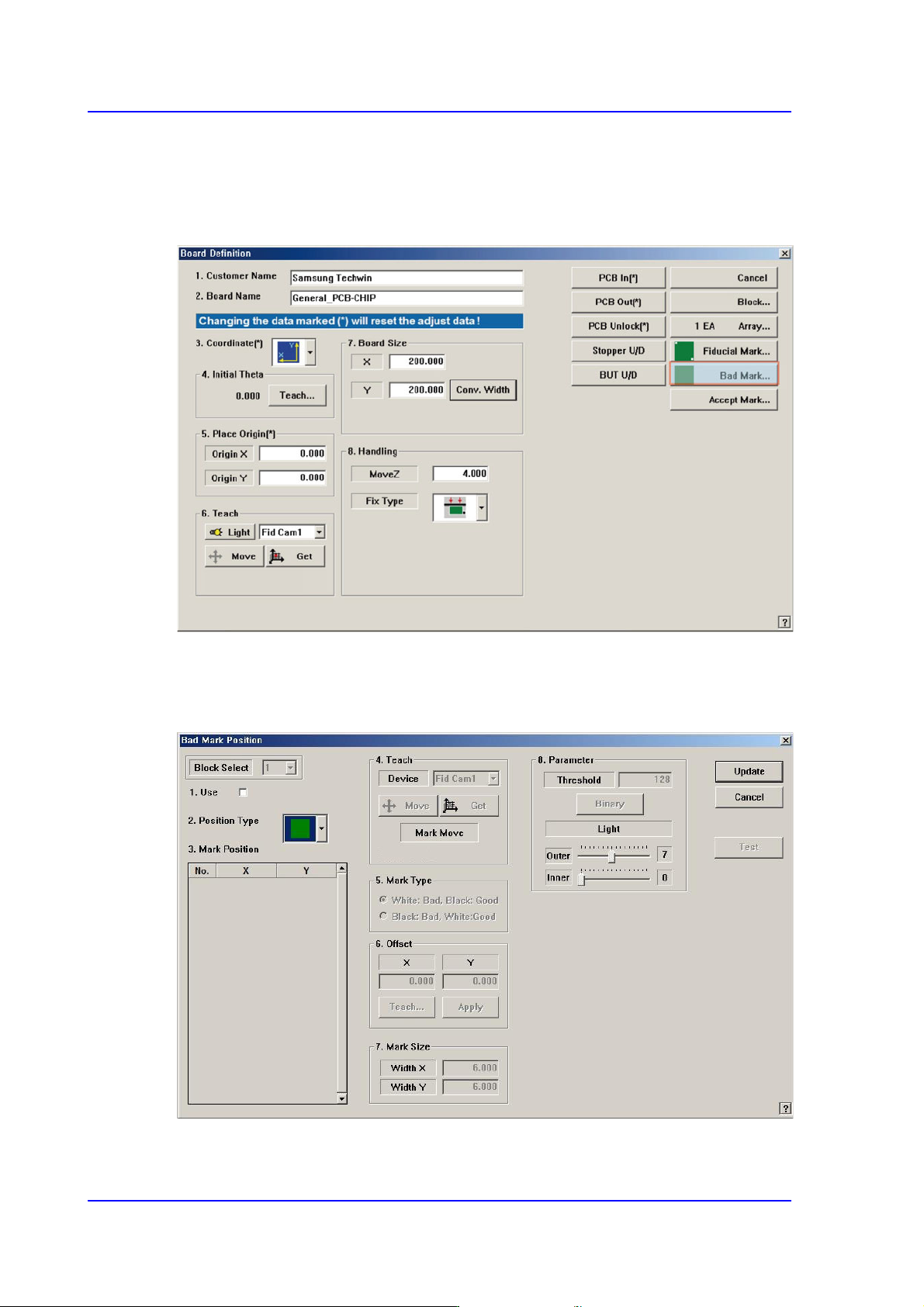
6-32 Multi-Functional Placer SM482( L) PLUS Administrator’s Guide 6.4. Bad Mark Setup The ‘Bad Mark’ refers to the mark indicated on the PCB to show whether a small PCB in the array PCB is good or defec tive. Pla cement …
6-31
Board Definition
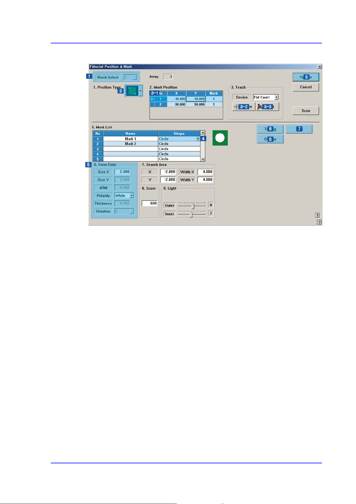
6.3.1. Fiducial Mark Setup Order
1) Block Setup
Omitted for non-block PC
2) Position Type’ setup
3) Mark Position’ setup
Select a fiducial mark in the <Mark Position> group.
Click the <Move> button to move the fiducial camera to the selected fiducial mark.
Perform adjustments so that the center of the fiducial mark falls on the crosshair center
of the SMVision window.
Click the <Get> button to input the coordinate of the fiducial mark.
4) ‘Mark List’ setup
5) ‘Form Data’ setup
6) Outline check
Click the <Outline> button to check if the outline seen in the SMVision window falls
on the fiducial mark outline.
If not, revise the “Shape Information’.
7) Fiducial mark recognition test
8) Tuning
Perform tuning at least more than twice.
9) Reflect set value: Click the <Update> button
6-32
Multi-Functional Placer SM482(L) PLUS Administrator’s Guide
6.4. Bad Mark Setup
The ‘Bad Mark’ refers to the mark indicated on the PCB to show whether a small PCB in
the array PCB is good or defective. Placement is not performed on the small PCB
indicated defective.
When this <Bad Mark…> button is clicked on, the following dialog box to edit bad mark
data is displayed.
Figure6.6 “Bad Mark Position” dialog box (When the Position Type is “None”)
6-33
Board Definition
<Block Select> combo box
For a Multi PCB
The model selected from the “Board Definition” dialog box is selected
automatically and the corresponding Combo Box is disabled..
For a Block PCB
Select the model for which setup will be performed and set other items.
<1.Use> check box
Determines whether to use a bad mark.
<2. Position Type> combo box
Select a bad mark type. The bad marks that can be selected are as follow;
None: Bad Mark.
Teach the bad mark on the first small PCB and determine the position of the bad
marks on each small PCB using the array offset that was already set up.
Set the bad mark offset to determine the bad mark positions automatically.
<3. Mark Position> group
If “None” is not selected in the <2. Position Type> combo box, data is created
according to the selected recognition type. The number of data generated is as follows;
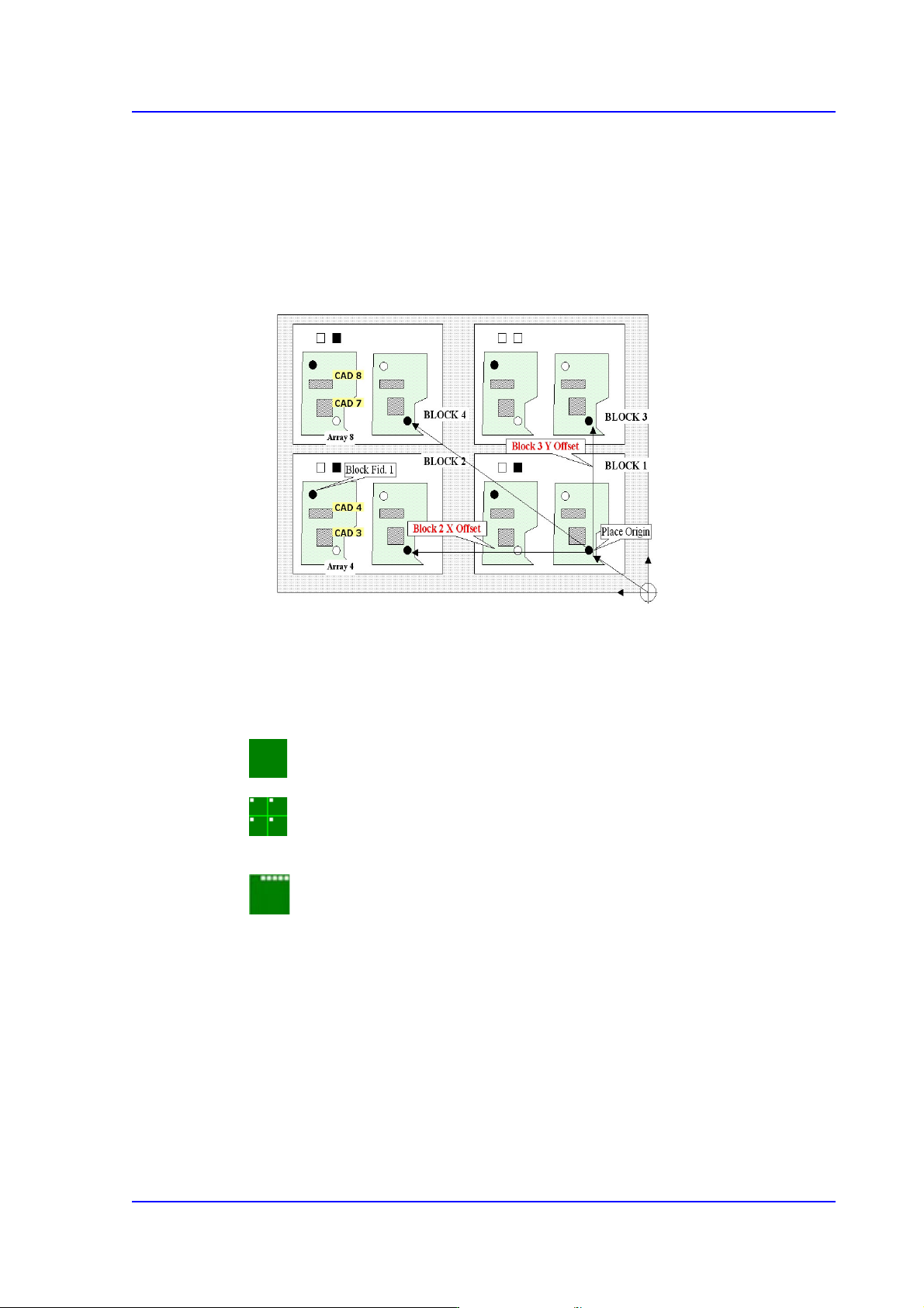
When the <Position Type> is “Array”: 1
For example, when “Array” is selected in <2. Position Type> combo box, the
following dialog box is displayed. (When the number of Array PCBs is 4)