Administrator’s Guide(CP45FV) Eng.pdf - 第220页
Samsung Component Placer CP45FV Administrator ’ s Guide After checking the listed contents of the erro r , take proper action. If the pr ogram is prepared properly , the PCB Download Error does not occur as shown below .…
Placement Test
14-5
PCB Edit Finish
Click the <Finish> submenu to conclude the PCB Edit.
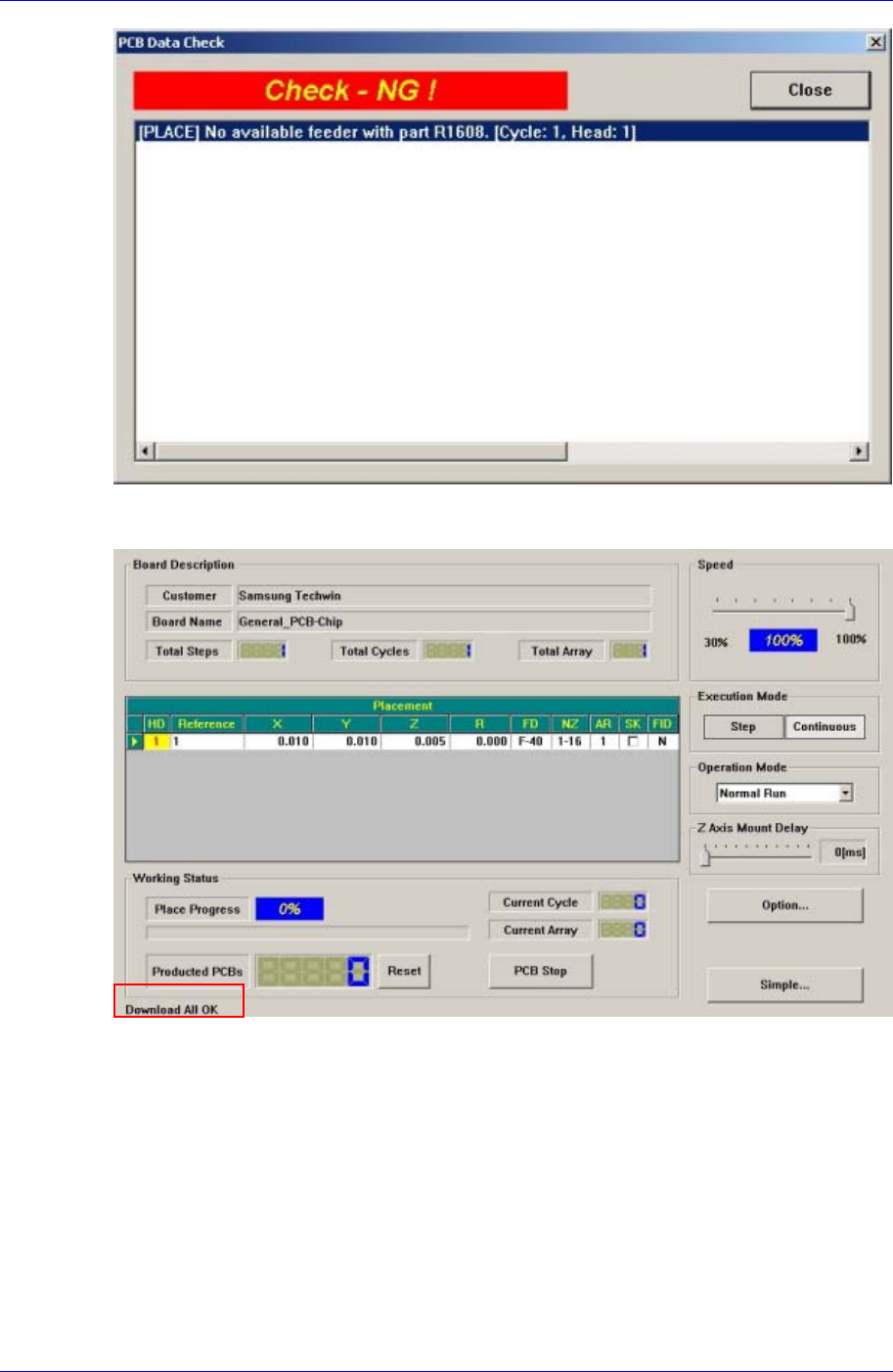
PCB File Downloading
Click the <PCB D/L> submenu to download the completed PCB file to the machine.
If there is no problem with the PCB file data, “Download All OK” is indicated at the
bottom of the screen.
If the <Detail…> button is clicked in the <Production> dialog box, a more detailed
screen is displayed.
Start
If there is no problem with the download and other PCB data, click <Start> after
completing all other preparation works and then press the <Start> button on the front
control panel.
14.3. Measures against Error during Placement Test
When error occurs during placement, stop the machine temporarily to examine the cause
of error for proper action and begin the work again.
The type of generally occurring errors includes PCB File Load Error, Fiducial Mark
Recognition Error, Component Pickup Error, Component Recognition Error and
Component Placement Error.
Warning
Adjusting the sensor or correcting an error while the
machine is ready could result in personal injury.
Be sure to adjust the sensor or correct an error in the stop
status (idle mode) after canceling the ready status.
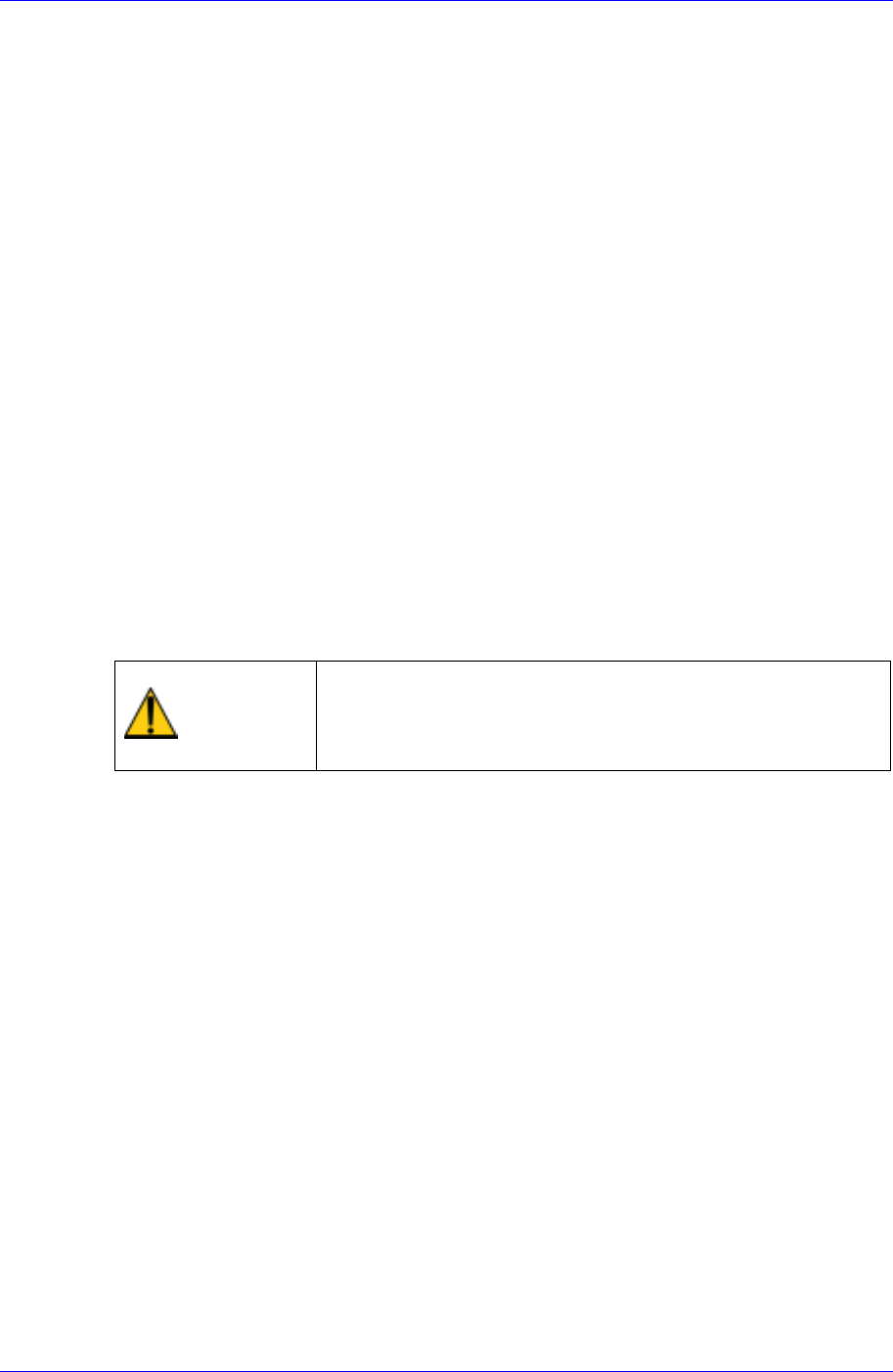
14.3.1. PCB File Download Error
Click the <PCB D/L> submenu on the left of the screen in the production menu to
download a PCB file. If an error occurs during this process, the following message
window is displayed.
Samsung Component Placer CP45FV Administrator’s Guide
After checking the listed contents of the error, take proper action. If the program is
prepared properly, the PCB Download Error does not occur as shown below.
The above screen shows the dialog box that is displayed after clicking the <Detail…>
button in the <Production> dialog box.
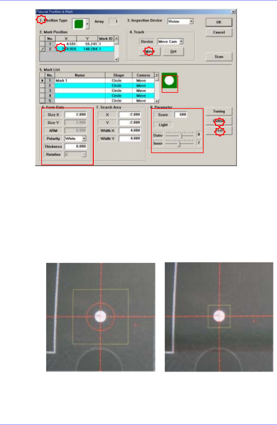
14.3.2. Fiducial Mark Recognition Error
This refers to the error occurred since the fiducial mark on the PCB cannot be recognized.
When such an error occurs, check the data related to the fiducial mark in the board dialog
box and examine the cause of the error through the recognition test to take proper
measure.
14-6
Placement Test
14-7
Check if the position type selected from the <1. Position Type> is identical to that of
the fiducial mark on the PCB, and also check if the shapes of the fiducial marks are
identical.
Select the coordinate of the position of the fiducial mark in the <2. Mark Position>
group and click the <Move> button in the <4. Teach> group to check the shape of the
fiducial mark selected through the vision monitor.
If the fiducial mark is not seen clearly, adjust the brightness of the lighting in the <8.
Parameter> group to make it clearer.
Click the <Outline> button to ensure that the shapes of the set fiducial mark and
actual fiducial mark are identical. If not, adjust the data in the <6. Form Data> to
make them identical.
<Outline and Fiducial Mark not Identical> <Outline and Fiducial Mark Identical>
Lastly, click the <Test> button to perform the fiducial mark recognition test.
By using the registered mark information, finds the exact size of the mark.