Administrator’s Guide(CP45FV) Eng.pdf - 第80页
Samsung Component Placer CP45FV Series Administrator ’ s Guide T each the first position of the bad mark. When the “ Enter ” key is pressed after teaching, the following screen is displayed. T each the position of the ne…
Board Definition
6-19
driving shafts of the X and Y motors or obtains the current coordinate of the
device to be selected. Available devices are as follows;
Move Cam: Selects the teaching camera.
Head1: : Selects Head1.
Head2: : Selects Head2.
Head3: : Selects Head3.
Head4: : Selects Head4.
Head5: : Selects Head5.
Head6: : Selects Head6.
Beam: Selects Beam.
<Move> button
Moves the head assembly by rotating the shafts of the X and Y-axes driving
motors using the device selected from the <Device> combo box. Before
executing “Move, the cell in the grid corresponding to the desired position
must be clicked on with a mouse.
<Get> button
Reads in the current position of the XY axis of the device selected in
<Device>. Before executing, “Get”, the cell in the grid corresponding to the
desired position must be clicked on with a mouse.
<6. Logic> group
Select the color of bad mark. Available colors of bad marks are as follows.
Black: the mark looks darker than the surroundings.
White: the mark looks lighter than the surroundings.
<7. Offset> group
Used to set the offset value between bad marks automatically.
<X> edit box
Set the offset value of X.
<Y> edit box
Set the offset value of Y.
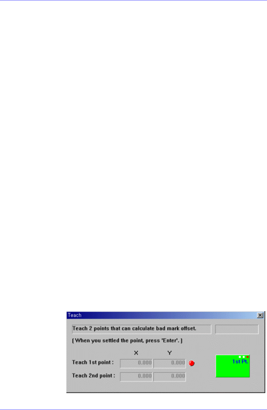
<Teach> button
Teach the offset value of bad mark by using the same method as teaching the
PCB size. When this button is clicked on, the following screens are displayed
in succession.
Samsung Component Placer CP45FV Series Administrator’s Guide
Teach the first position of the bad mark. When the “Enter” key is pressed
after teaching, the following screen is displayed.
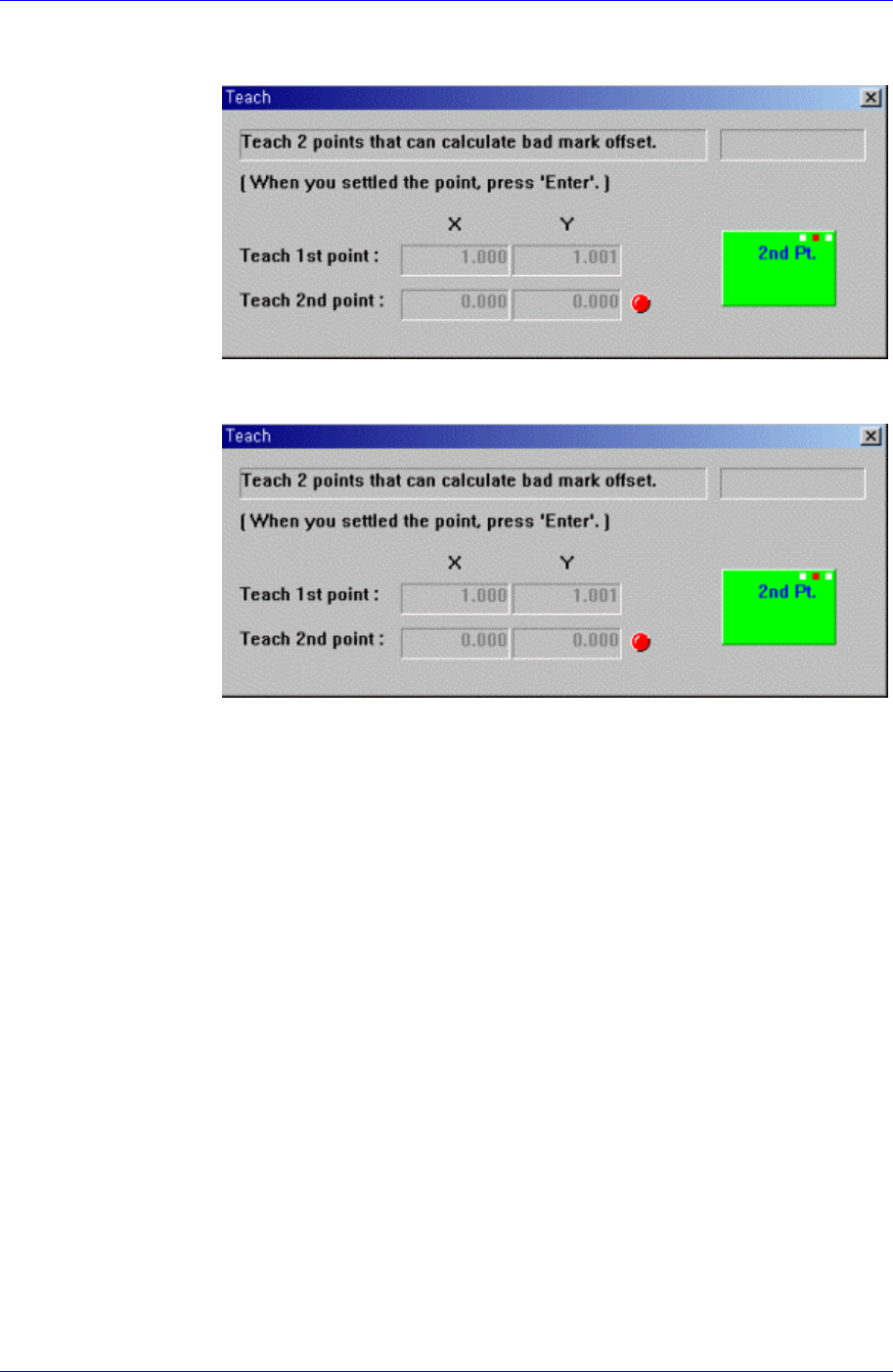
Teach the position of the neighboring bad mark. When the “Enter” key is
pressed after teaching, the following screen is displayed.
Press the “Enter” key to complete the bad mark offset value teaching
operation.
<Apply> button
Automatically creates the bad mark position data by using the offset value set
in this group.
<8. Camera No.> combo box
Select the camera to search the bad mark. At present, it is fixed to “Move
Camera(Fiducial Camera)”.
<9. Mark Size> group
Set the area in which to search the bad mark. The main purpose of this feature is
to limit the search range for when there are forms similar to the mark near the
mark such that they can interfere with recognition on certain PCBs.
<Width X> edit box
Set the value of search range in X axis direction. In general, it is 6 mm.
<Width Y> edit box
Set the value of search range in Y axis direction. In general, it is 6 mm.
<10. Parameter> group
<Threshold> edit box
Sets the threshold value determining whether the image pixel is black or
white when inspecting the bad mark. For example, if <Bad Mark> is “Black”
and the <Threshold> value is 100, then all the values under 100 in the vision
6-20
Board Definition
6-21
image are recognized as black, and if <Bad Mark> is “White” and the
<Threshold> value is 100, then all values over 100 are recognized as white.
<Light> group
Set the light value for bad mark inspection. In general it is 7, but adjust it
appropriately according to the condition of PCB and bad mark.
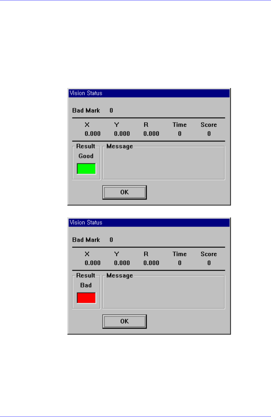
<Test> button
By using the registered mark information, tests the mark.. The accuracy of
the registered mark data can be verified. When the test is successful, the
following message box is displayed.
When the test is not successful, the following message box is displayed.
<OK> button
Saves the bad mark data and closes the “Bad Position” dialog box.
<Cancel> button
Closes the “Bad Position” dialog box without saving the bad mark data.
<Accept Mark…> button
A bad mark is a mark that indicates whether a loaded PCB is good or defective. When
a PCB is defective, the bad mark is marked but the accept mark is not marked, and