sh030106u.pdf - 第113页
3. SIG NALS A ND WIRI NG 3 - 36 3.8.2 Det ailed expl anatio n of i nterfaces This sectio n provides the d etails of the I/O s ignal in terfaces (refer to the I/O divis io n in the table) giv en in section 3.5. Refer t o …
3. SIGNALS AND WIRING
3 - 35
3.8 Interfaces
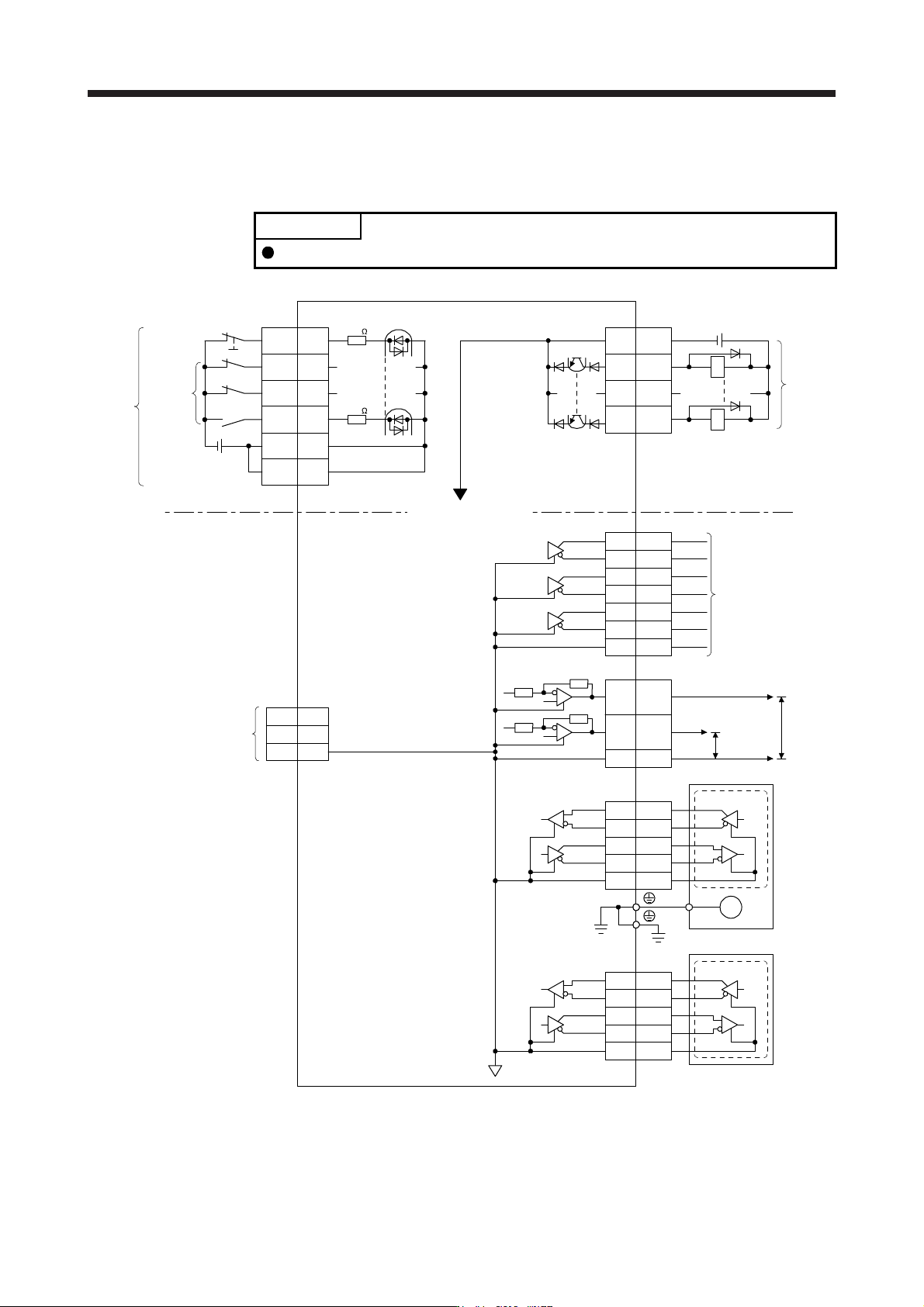
3.8.1 Internal connection diagram
POINT
Refer to section 13.3.1 for the CN8 connector.
3
CN3
6
16
7
17
8
18
LA
LAR
LB
LBR
LZ
LZR
2
4
7
8
MR
MRR
MX
MXR
LG
PE
M
CN2
CN3
MO1
MO2
LG
4
14
1
LG11
EM2
CN3
20
DI1 2
DI2 12
DI3 19
DICOM
5
10
CN3
3
13
9
15
DOCOM
INP
ALM
USB
D+
GND
D- 2
3
5
CN5
MBR
DICOM
RA
RA
3
2
4
7
8
MR2
MRR2
MX2
MXR2
LG
External encoder
(Note 4, 6) CN2L
±10 V DC
±10 V DC
Encoder
Differential line
driver output
(35 mA or less)
Servo motor
Analog monitor
(Note 2)
Servo amplifier
(Note 1)
24 V DC
Forced stop 2
(Note 3)
(Note 3)
Isolated
Approximately
6.2 k
Approximately
6.2 k
Encoder
(Note 5)
24 V DC
(Note 5)
Note 1. Signal can be assigned for these pins with the controller setting.
For contents of signals, refer to the instruction manual of the controller.
2. The signal cannot be used in the speed control mode and torque control mode.
3. This diagram shows sink I/O interface. For source I/O interface, refer to section 3.8.3.
4. This is for MR-J4-_B_-RJ servo amplifier. MR-J4-_B_ servo amplifier does not have CN2L connector.
5. The illustration of the 24 V DC power supply is divided between input signal and output signal for convenience. However, they
can be configured by one.
6. Refer to table 1.1 for connections of external encoders.
3. SIGNALS AND WIRING
3 - 36
3.8.2 Detailed explanation of interfaces
This section provides the details of the I/O signal interfaces (refer to the I/O division in the table) given in
section 3.5. Refer to this section and make connection with the external device.
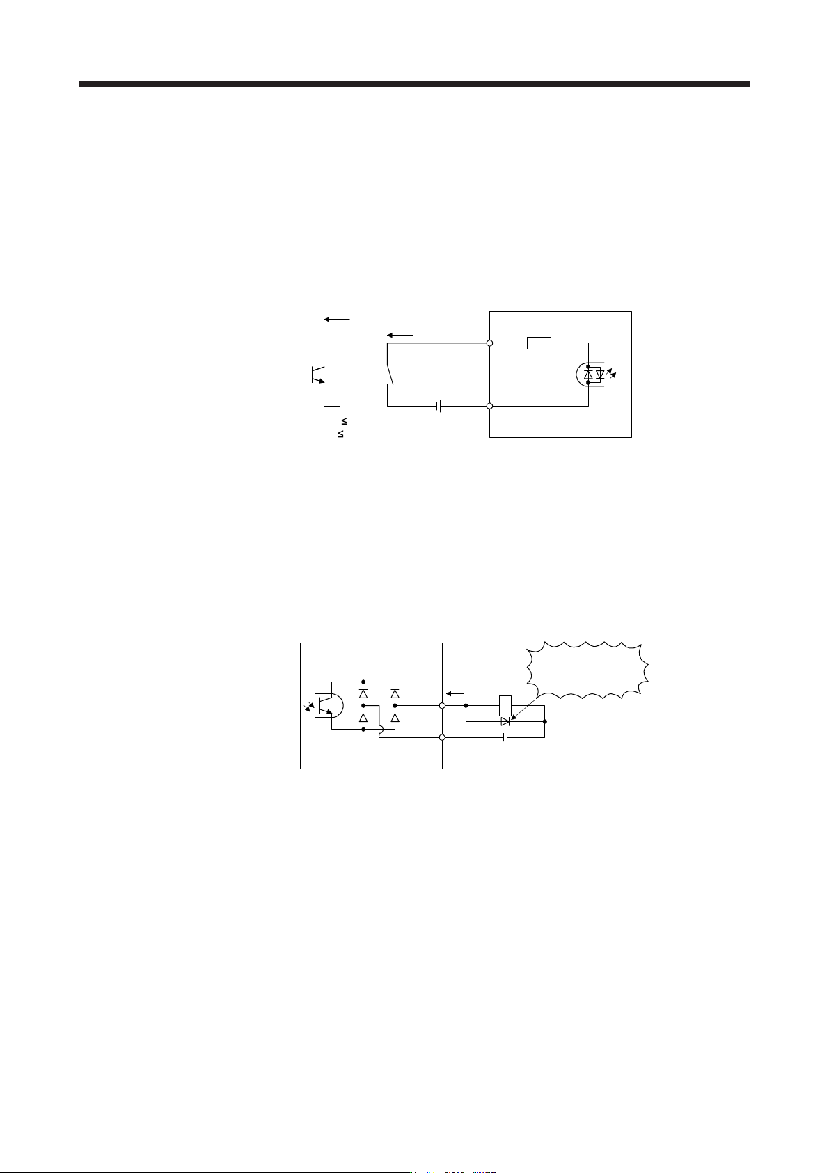
(1) Digital input interface DI-1
This is an input circuit whose photocoupler cathode side is the input terminal. Transmit signals from sink
(open-collector) type transistor output, relay switch, etc. The following is a connection diagram for sink
input. Refer to section 3.8.3 for source input.
Approximately
6.2 kΩ
Approximately
5 mA
V
CES
1.0 V
I
CEO
100 µA
TR
24 V DC ± 10%
300 mA
Switch
For transistor
EM2,
etc.
Servo amplifier
DICOM
(2) Digital output interface DO-1
This is a circuit in which the collector of the output transistor is the output terminal. When the output
transistor is turned on, the current will flow to the collector terminal.
A lamp, relay or photocoupler can be driven. Install a diode (D) for an inductive load, or install an inrush
current suppressing resistor (R) for a lamp load.
(Rated current: 40 mA or less, maximum current: 50 mA or less, inrush current: 100 mA or less) A
maximum of 2.6 V voltage drop occurs in the servo amplifier.
The following shows a connection diagram for sink output. Refer to section 3.8.3 for source output.
(Note) 24 V DC ± 10%
300 mA
If polarity of diode is
reversed, servo amplifier
will malfunction.
Servo amplifier
ALM,
etc.
Load
DOCOM
Note. If the voltage drop (maximum of 2.6 V) interferes with the relay operation, apply high
volta
g
e
(
maximum of 26.4 V
)
from external source.
3. SIGNALS AND WIRING
3 - 37
(3) Encoder output pulses DO-2 (differential line driver type)
(a) Interface
Maximum output current: 35 mA
150 Ω
100 ΩAm26LS32 or equivalent
Servo amplifier
LA
(LB, LZ)
LAR
(LBR, LZR)
SD
LG
High-speed photocoupler
Servo amplifier
LAR
(LBR, LZR)
SD
LA
(LB, LZ)
(b) Output pulse
/2
LAR
T
Servo motor CCW rotation
Time cycle (T) is determined by the settings of
[Pr. PA15] and [Pr. PC03].
LA
LB
LBR
LZ
LZR
400 µs or more
(4) Analog output
LG
MO1
(MO2)
Servo amplifier
Output voltage: ±10 V
Maximum output current: 1 mA
Resolution: 10 bits or equivalent
Note. Output volta
g
e ran
g
e varies dependin
g
on the output contents.