sh030106u.pdf - 第643页
APPENDIX App. - 12 (4) CN10 Device Symbol Pin No. Function/applicat ion I/O divi sion A-axi s shutdown 2 SDI2A+ SDI2A- 3A 3B Connect thi s device t o a safety s witch for A-ax is driving devic e. Input the s ame signal a…
APPENDIX
App. - 11
App. 5.8 Signal
App. 5.8.1 Connector/pin assignment
(1) CN8A
Device Symbol Pin No. Function/application
I/O
division
A-axis STO1 STO1A-
STO1A+
1
4
Outputs STO1 to A-axis driving device.
Outputs the same signal as A-axis STO2.
STO state (base shutdown): Between STO1A+ and STO1A- is opened.
STO release state (in driving): Between STO1A+ and STO1A- is closed.
O
A-axis STO2 STO2A-
STO2A+
5
6
Outputs STO2 to A-axis driving device.
Outputs the same signal as A-axis STO1.
STO state (base shutdown): Between STO2A+ and STO2A- is opened.
STO release state (in driving): Between STO2A+ and STO2A- is closed.
O
A-axis STO
state
TOF2A
TOF1A
7
8
Inputs STO state of A-axis driving device.
STO state (base shutdown): Open between TOF2A and TOF1A.
STO release state (in driving): Close between TOF2A and TOF1A.
I
(2) CN8B
Device Symbol Pin No. Function/application
I/O
division
B-axis STO1 STO1B-
STO1B+
1
4
Outputs STO1 to B-axis driving device.
Outputs the same signal as B-axis STO2.
STO state (base shutdown): Between STO1B+ and STO1B- is opened.
STO release state (in driving): Between STO1B+ and STO1B- is closed.
O
B-axis STO2 STO2B-
STO2B+
5
6
Outputs STO2 to B-axis driving device.
Outputs the same signal as B-axis STO1.
STO state (base shutdown): Between STO2B+ and STO2B- is opened.
STO release state (in driving): Between STO2B+ and STO2B- is closed.
O
B-axis STO
state
TOF2B
TOF1B
7
8
Inputs STO state of B-axis driving device.
STO state (base shutdown): Open between TOF2B and TOF1B.
STO release state (in driving): Close between TOF2B and TOF1B.
I
(3) CN9
Device Symbol Pin No. Function/application
I/O
division
A-axis
shutdown 1
SDI1A+
SDI1A-
1A
1B
Connect this device to a safety switch for A-axis driving device.
Input the same signal as A-axis shutdown 2.
STO state (base shutdown): Open between SDI1A+ and SDI1A-.
STO release state (in driving): Close between SDI1A+ and SDI1A-.
DI-1
B-axis
shutdown 1
SDI1B+
SDI1B-
2A
2B
Connect this device to a safety switch for B-axis driving device.
Input the same signal as B-axis shutdown 2.
STO state (base shutdown): Open between SDI1B+ and SDI1B-.
STO release state (in driving): Close between SDI1B+ and SDI1B-.
DI-1
A-axis SDO1 SDO1A+
SDO1A-
4A
4B
Outputs STO1 to A-axis driving device.
Outputs the same signal as A-axis SDO2.
STO state (base shutdown): Between SDO1A+ and SDO1A- is opened.
STO release state (in driving): Between SDO1A+ and SDO1A- is closed.
DO-1
B-axis SDO1 SDO1B+
SDO1B-
3A
3B
Outputs STO1 to B-axis driving device.
Outputs the same signal as B-axis SDO2.
STO state (base shutdown): Between SDO1B+ and SDO1B- is opened.
STO release state (in driving): Between SDO1B+ and SDO1B- is closed.
DO-1
APPENDIX
App. - 12
(4) CN10
Device Symbol
Pin
No.
Function/application
I/O
division
A-axis
shutdown 2
SDI2A+
SDI2A-
3A
3B
Connect this device to a safety switch for A-axis driving device.
Input the same signal as A-axis shutdown 1.
STO state (base shutdown): Open between SDI2A+ and SDI2A-.
STO release state (in driving): Close between SDI2A+ and SDI2A-.
DI-1
B-axis
shutdown 2
SDI2B+
SDI2B-
4A
4B
Connect this device to a safety switch for B-axis driving device.
Input the same signal as B-axis shutdown 1.
STO state (base shutdown): Open between SDI2B+ and SDI2B-.
STO release state (in driving): Close between SDI2B+ and SDI2B-.
DI-1
A-axis EMG
start/reset
SRESA+
SRESA-
1A
1B
Signal for releasing STO state (base shutdown) on A-axis driving device.
Releases STO state (base shutdown) on A-axis driving device by switching between
SRESA+ and SRESA- from on (connected) to off (opened).
DI-1
B-axis EMG
start/reset
SRESB+
SRESB-
2A
2B
Signal for releasing STO state (base shutdown) on B-axis driving device.
Releases STO state (base shutdown) on B-axis driving device by switching between
SRESB+ and SRESB- from on (connected) to off (opened).
DI-1
A-axis SDO2 SDO2A+
SDO2A-
6A
6B
Outputs STO2 to A-axis driving device.
Outputs the same signal as A-axis STO1.
STO state (base shutdown): Between SDO2A+ and SDO2A- is opened.
STO release state (in driving): Between SDO2A+ and SDO2A- is closed.
DO-1
B-axis SDO2 SDO2B+
SDO2B-
5A
5B
Outputs STO2 to B-axis driving device.
Outputs the same signal as B-axis SDO1.
STO state (base shutdown): Between SDO2B+ and SDO2B- is opened.
STO release state (in driving): Between SDO2B+ and SDO2B- is closed.
DO-1
Control circuit
power supply
+24V 7A Connect + side of 24 V DC.
Control circuit
power GND
0V 7B Connect - side of 24 V DC.
A-axis STO
state
TOFA 8A TOFA is internally connected with TOF2A.
B-axis STO
state
TOFB 8B TOFB is internally connected with TOF2B.
App. 5.8.2 Interfaces
In this servo amplifier, source type I/O interfaces can be used.
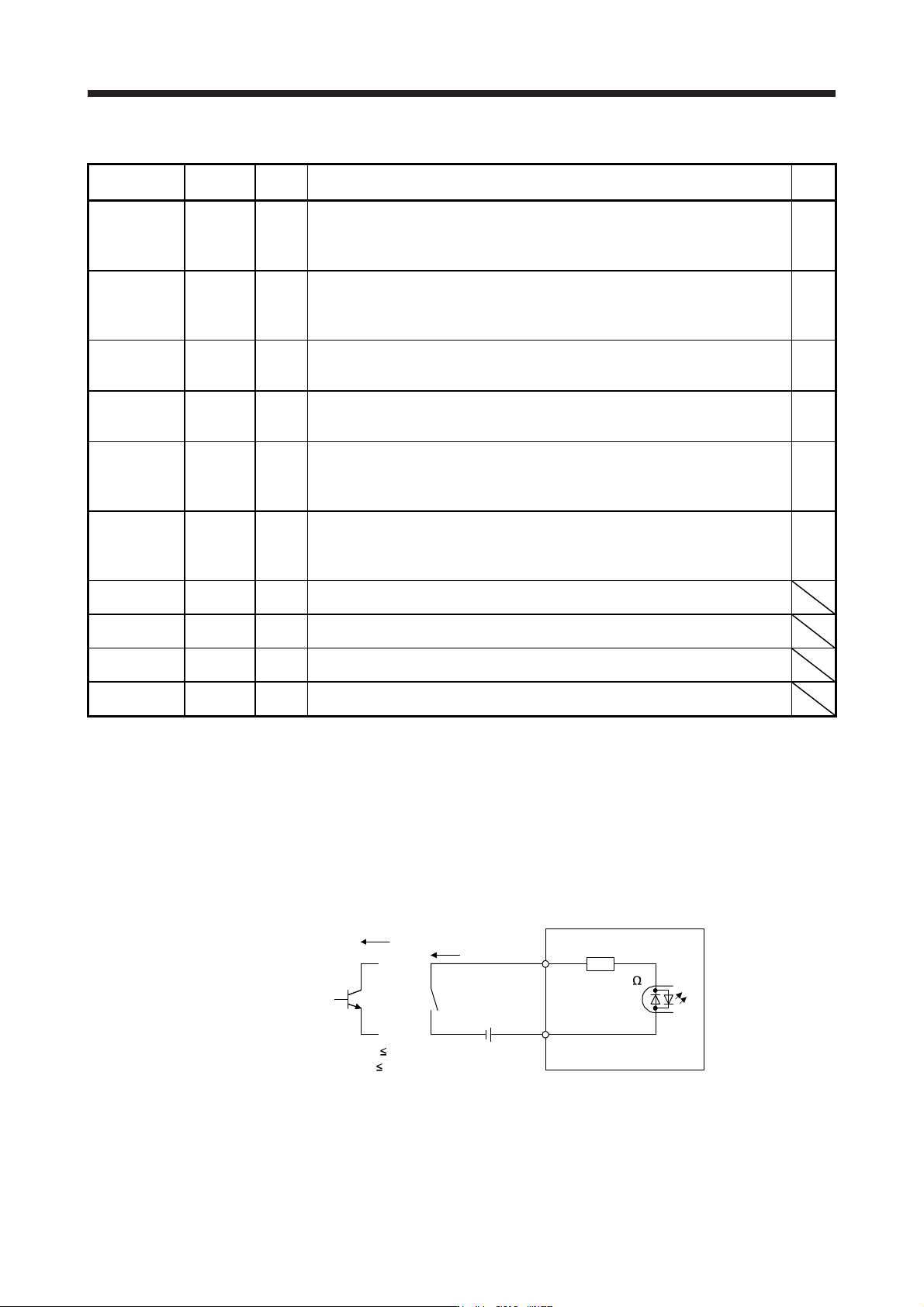
(1) Sink I/O interface (CN9, CN10 connector)
(a) Digital input interface DI-1
This is an input circuit whose photocoupler cathode side is the input terminal. Transmit signals from
sink (open-collector) type transistor output, relay switch, etc.
V
CES
1.0 V
I
CEO
100 µA
24 V DC ± 10%
200 mA
Approx. 5.4 k
Approximately
5 mA
TR
Switch
For transistor
SRESA-,
etc.
MR-J3-D05
SRESA+,
etc.
APPENDIX
App. - 13
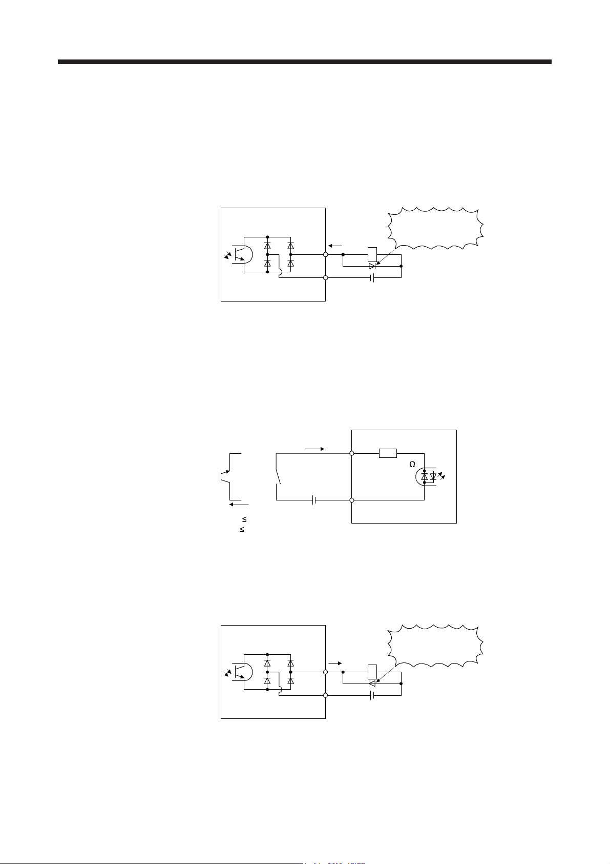
(b) Digital output interface DO-1
This is a circuit in which the collector of the output transistor is the output terminal. When the output
transistor is turned on, the current will flow to the collector terminal.
A lamp, relay, or photocoupler can be driven. Install a diode (D) for an inductive load, or install an
inrush current suppressing resistor (R) for a lamp load. (Rated current: 40 mA or less, maximum
current: 50 mA or less, inrush current: 100 mA or less) A maximum of 2.6 V voltage drop occurs in
the MR-J3-D05.
If polarity of diode is
reversed, MR-J3-D05
will malfunction.
(Note) 24 V DC ± 10%
200 mA
MR-J3-D05
SDO2B+,
etc.
SDO2B-,
etc.
Load
Note. If the voltage drop (maximum of 2.6 V) interferes with the relay operation, apply high
volta
g
e
(
maximum of 26.4 V
)
from external source.
(2) Source I/O interfaces (CN9, CN10 connector)
(a) Digital input interface DI-1
This is an input circuit whose photocoupler anode side is the input terminal. Transmit signals from
source (open-collector) type transistor output, relay switch, etc.
V
CES
1.0 V
I
CEO
100 µA
Approximately 5 mA
24 V DC ± 10%
200 mA
Switch
SRESA-,
etc.
MR-J3-D0
5
SRESA+,
etc.
Approx. 5.4 k
(b) Digital output interface DO-1
This is a circuit in which the emitter of the output transistor is the output terminal. When the output
transistor is turned on, current will be applied from the output to a load. A maximum of 2.6 V voltage
drop occurs in the MR-J3-D05.
MR-J3-D05
If polarity of diode is
reversed, MR-J3-D05
will malfunction.
(Note) 24 V DC ± 10%
200 mA
Load
SDO2B+,
etc.
SDO2B-,
etc.
Note. If the voltage drop (maximum of 2.6 V) interferes with the relay operation, apply high
volta
g
e
(
maximum of 26.4 V
)
from external source.