sh030106u.pdf - 第644页
APPENDIX App. - 13 (b) Dig ital ou tput interfac e DO-1 This is a c ircuit in w hich the c ollector of t he outp ut trans ist or is the output term inal. Wh en the o utput transistor is tur ned on, the curr ent will flo …
APPENDIX
App. - 12
(4) CN10
Device Symbol
Pin
No.
Function/application
I/O
division
A-axis
shutdown 2
SDI2A+
SDI2A-
3A
3B
Connect this device to a safety switch for A-axis driving device.
Input the same signal as A-axis shutdown 1.
STO state (base shutdown): Open between SDI2A+ and SDI2A-.
STO release state (in driving): Close between SDI2A+ and SDI2A-.
DI-1
B-axis
shutdown 2
SDI2B+
SDI2B-
4A
4B
Connect this device to a safety switch for B-axis driving device.
Input the same signal as B-axis shutdown 1.
STO state (base shutdown): Open between SDI2B+ and SDI2B-.
STO release state (in driving): Close between SDI2B+ and SDI2B-.
DI-1
A-axis EMG
start/reset
SRESA+
SRESA-
1A
1B
Signal for releasing STO state (base shutdown) on A-axis driving device.
Releases STO state (base shutdown) on A-axis driving device by switching between
SRESA+ and SRESA- from on (connected) to off (opened).
DI-1
B-axis EMG
start/reset
SRESB+
SRESB-
2A
2B
Signal for releasing STO state (base shutdown) on B-axis driving device.
Releases STO state (base shutdown) on B-axis driving device by switching between
SRESB+ and SRESB- from on (connected) to off (opened).
DI-1
A-axis SDO2 SDO2A+
SDO2A-
6A
6B
Outputs STO2 to A-axis driving device.
Outputs the same signal as A-axis STO1.
STO state (base shutdown): Between SDO2A+ and SDO2A- is opened.
STO release state (in driving): Between SDO2A+ and SDO2A- is closed.
DO-1
B-axis SDO2 SDO2B+
SDO2B-
5A
5B
Outputs STO2 to B-axis driving device.
Outputs the same signal as B-axis SDO1.
STO state (base shutdown): Between SDO2B+ and SDO2B- is opened.
STO release state (in driving): Between SDO2B+ and SDO2B- is closed.
DO-1
Control circuit
power supply
+24V 7A Connect + side of 24 V DC.
Control circuit
power GND
0V 7B Connect - side of 24 V DC.
A-axis STO
state
TOFA 8A TOFA is internally connected with TOF2A.
B-axis STO
state
TOFB 8B TOFB is internally connected with TOF2B.
App. 5.8.2 Interfaces
In this servo amplifier, source type I/O interfaces can be used.
(1) Sink I/O interface (CN9, CN10 connector)
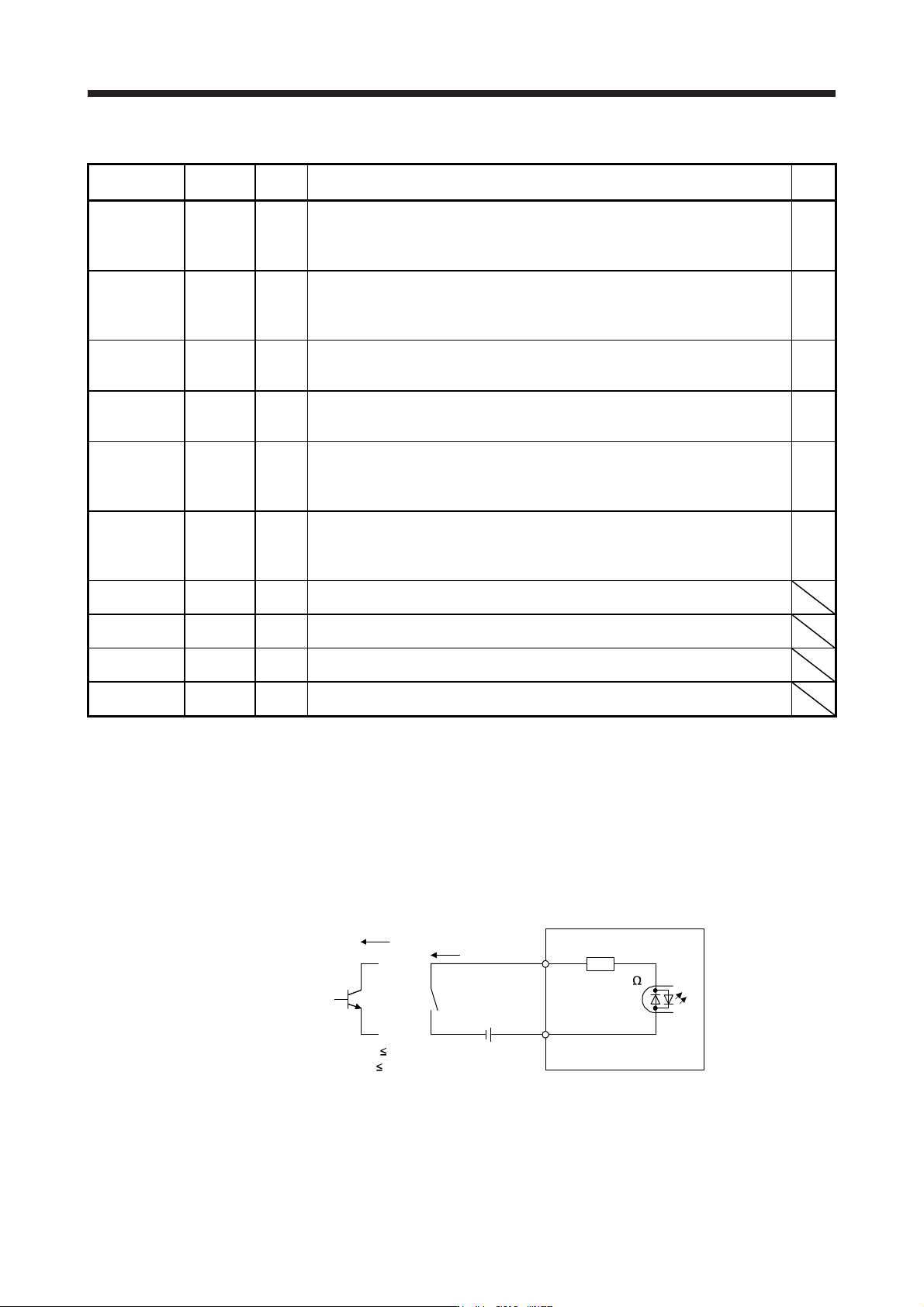
(a) Digital input interface DI-1
This is an input circuit whose photocoupler cathode side is the input terminal. Transmit signals from
sink (open-collector) type transistor output, relay switch, etc.
V
CES
1.0 V
I
CEO
100 µA
24 V DC ± 10%
200 mA
Approx. 5.4 k
Approximately
5 mA
TR
Switch
For transistor
SRESA-,
etc.
MR-J3-D05
SRESA+,
etc.
APPENDIX
App. - 13
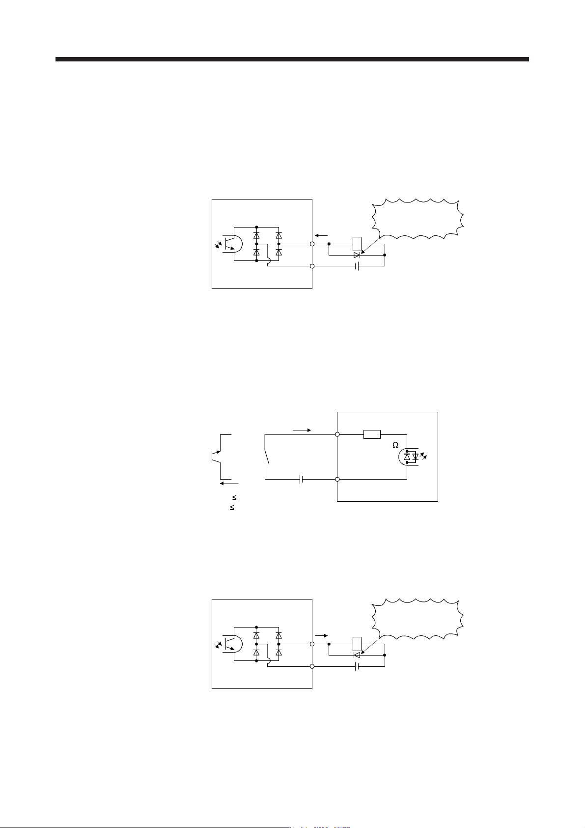
(b) Digital output interface DO-1
This is a circuit in which the collector of the output transistor is the output terminal. When the output
transistor is turned on, the current will flow to the collector terminal.
A lamp, relay, or photocoupler can be driven. Install a diode (D) for an inductive load, or install an
inrush current suppressing resistor (R) for a lamp load. (Rated current: 40 mA or less, maximum
current: 50 mA or less, inrush current: 100 mA or less) A maximum of 2.6 V voltage drop occurs in
the MR-J3-D05.
If polarity of diode is
reversed, MR-J3-D05
will malfunction.
(Note) 24 V DC ± 10%
200 mA
MR-J3-D05
SDO2B+,
etc.
SDO2B-,
etc.
Load
Note. If the voltage drop (maximum of 2.6 V) interferes with the relay operation, apply high
volta
g
e
(
maximum of 26.4 V
)
from external source.
(2) Source I/O interfaces (CN9, CN10 connector)
(a) Digital input interface DI-1
This is an input circuit whose photocoupler anode side is the input terminal. Transmit signals from
source (open-collector) type transistor output, relay switch, etc.
V
CES
1.0 V
I
CEO
100 µA
Approximately 5 mA
24 V DC ± 10%
200 mA
Switch
SRESA-,
etc.
MR-J3-D0
5
SRESA+,
etc.
Approx. 5.4 k
(b) Digital output interface DO-1
This is a circuit in which the emitter of the output transistor is the output terminal. When the output
transistor is turned on, current will be applied from the output to a load. A maximum of 2.6 V voltage
drop occurs in the MR-J3-D05.
MR-J3-D05
If polarity of diode is
reversed, MR-J3-D05
will malfunction.
(Note) 24 V DC ± 10%
200 mA
Load
SDO2B+,
etc.
SDO2B-,
etc.
Note. If the voltage drop (maximum of 2.6 V) interferes with the relay operation, apply high
volta
g
e
(
maximum of 26.4 V
)
from external source.
APPENDIX
App. - 14
App. 5.8.3 Wiring CN9 and CN10 connectors
Handle with the tool with care when connecting wires.
(1) Wire strip
(a) Use wires with size of AWG 24 to 20 (0.22 mm
2
to 0.5 mm
2
) (recommended electric wire: UL1007)
and strip the wires to make the stripped length 7.0 mm ± 0.3 mm. Confirm the stripped length with
gauge, etc. before using the wires.
(b) If the stripped wires are bent, loose or too thick due to twisting too much, fix the wires by twisting
lightly, etc. Then, confirm the stripped length before using the wires. Do not use excessively
deformed wires.
(c) Smooth out the wire surface and stripped insulator surface.
(2) Connecting wires
Before connecting wires, be sure to pull out the receptacle assembly from the header connector. If wires
are connected with inserted connector, the connector and the printed board may malfunction.
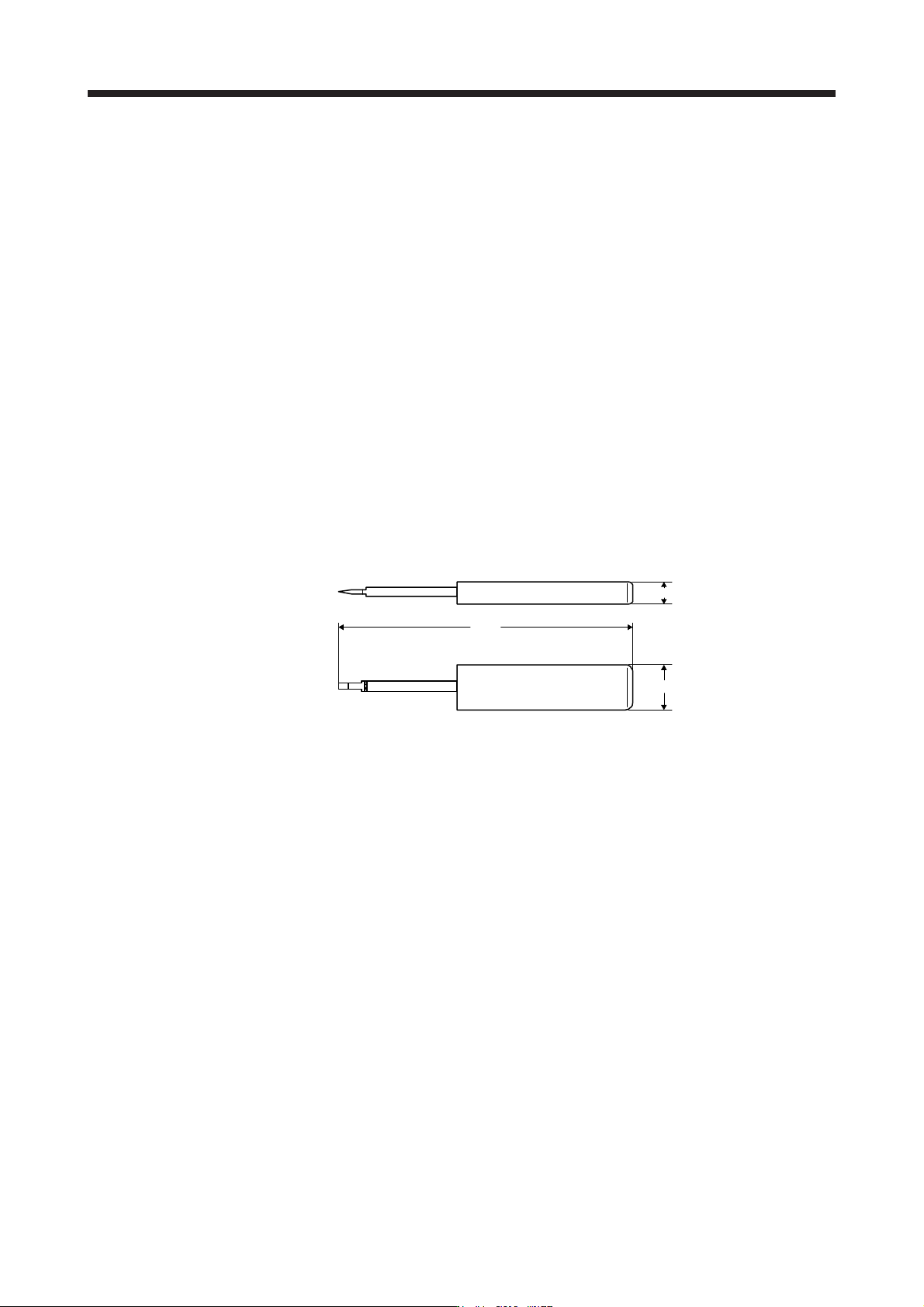
(a) Using extraction tool (1891348-1 or 2040798-1)
1) Dimensions and mass
[Unit: mm]
100
15
7
Mass: Approx. 20 g