operation-cp45.pdf - 第160页
Samsung Component Placer CP-45F(V)/FS Operations Manual 11-6 Select the method for PCB arrangement. Hole Fixer : A method of arrangement by inserting the pins i n the holes of the PCB. Edge Fixer: A m ethod of arrangemen…
PCB Edit Command
11-5
Moves the XY and Z axes to the device specified in <Device>. At this time, the
position value to be read is the origin or Move Z. Before executing “Move”, the
edit box corresponding to the desired position value must be clicked on with a
mouse.
<Get> button
Reads in the current position of the XY and Z axes of the device selected in
<Device>. At this time, the target position value to get is the origin or Move Z,
before executing “Get”, the edit box corresponding to the desired position must
be clicked on with a mouse.
<7. Board Size> group
Set the board size.
<X> edit box
Set the X value of PCB size
<Y> edit box
Set the Y value of PCB size.
<Z> edit box
Set the Z value(thickness) of PCB size.
The sizes of PCB applicable for this equipment are as follows.
Front side conveyor fixed
Max: 460L×400W×4.2H [ mm ]
510.0mm (x-axis) x 460.0mm (y-axis) – Factory Option
Min: 50L×50W×0.38H [ mm ]
The maximum PCB size could differ according to the options.
20 stages Tray Feeder : 460 × 350 (2Tray / 1Pallet) , 460 × 400 (1Tray / 1Pallet)
24 stages Tray Feeder : 460 × 300 (1Tray / 1Pallet)
Rear side conveyor fixed
Max: 410L×360W×4.2H [ mm ]
Min: 50L×50W×0.38H [ mm ]
The maximum PCB size could differ according to the options.
20 stages Tray Feeder : 460 × 300 less
24 stages Tray Feeder : 460 × 270 less
<8. Handling> group
Set the data necessary for PCB operation.
<Fix Type> combo box
Memo
Samsung Component Placer CP-45F(V)/FS Operations Manual
11-6
Select the method for PCB arrangement.
Hole Fixer: A method of arrangement by inserting the pins in the holes of
the PCB.
Edge Fixer: A method of arrangement by pushing the PCB from the side
with a device attached on the conveyor.
Edge Fixer2: : It is the same as the “Edge Fixer” method, but it is a
method of pushing twice from the side.
<Wait Type> combo box
Select the waiting position of the head block when the PCB board is loaded
Auto: the equipment determines the waiting position automatically.
System: waiting at the position specified by the system.
<Move Z>
Set the minimum distance between the top of the PCB and the end of the head (if
a nozzle is attached, to the end of the nozzle) during PCB operation.
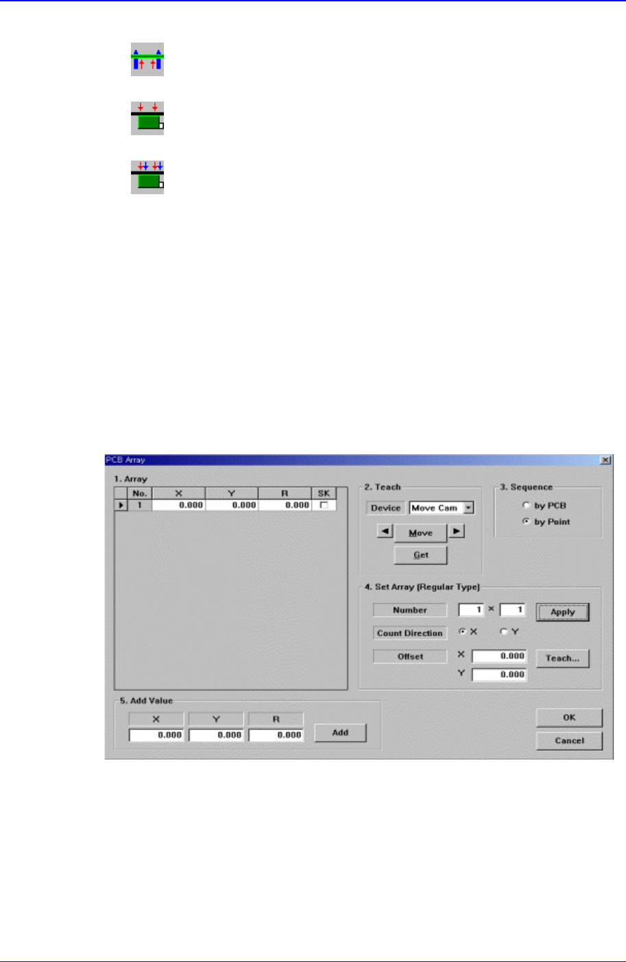
<Array…> button
If the Array PCB is more than one, set the offset value between the origin of each
Array PCB and the placement origin of PCB. When this button is clicked on, the
following dialog box is displayed.
Figure 11-8. “PCB Array” dialog box
<1. Array> group
Set the offset value of Array PCB from the “Place Origin” of the PCB.
<2. Teach> group
Used to move the XY and R axes of the equipment to the specified position or to
read in the current position of the XY and R axes.
<Device> combo box
To move or to read in the position of the XY and R axes, select the
PCB Edit Command
11-7
corresponding device. Available devices are as follows.
Move Cam: Selects Teaching Camera.
Head1: Selects Head1.
Head2: Selects Head 2.
Head3: Selects Head 3.
Head4: Selects Head 4.
Head5: Selects Head 5.
Head6: Selects Head 6.
Beam: Selects Beam.
<Move> button
Moves the XY and R axes to the device selected in <Device>. Before
executing “Move”, the cell in the grid corresponding to the desired position
must be clicked on with a mouse.
<Get> button
Reads in the current position of the XY, and R axes of the device selected in
<Device>. Before executing “Move”, the cell in the grid corresponding to the
desired position must be clicked on with a mouse.
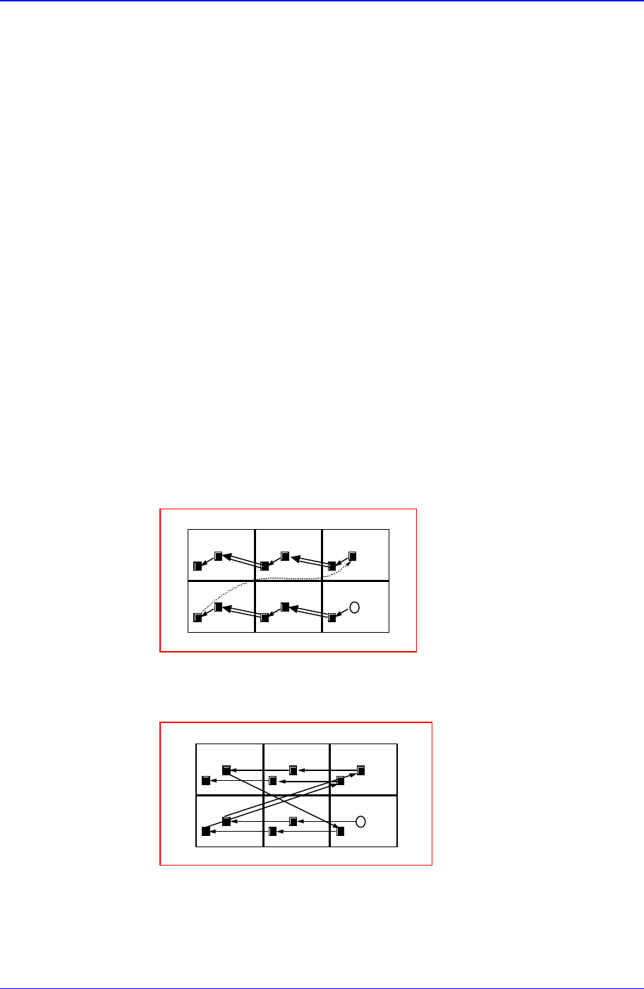
<3. Sequence> group
Select the Array PCB operation method.
<By PCB> option button
A method of completing one Array PCB operation and then executing the
next Array PCB operation.
13
4
2
56
<By Point> option button
A method of completing an operation cycle to all array PCBs and then
executing the next cycle operation.
13
4
2
56
<4. Set Array (Regular Type)> group
Initializes the Array PCB. This function sets the offset value of each Array PCB
automatically when the arrangement of array PCB is regular.
<Number> edit box group