operation-cp45.pdf - 第214页
Samsung Component Placer CP-45F(V)/FS Operations Manual 11-60 Figur e 1 1-39. “ Align T ype = V ision, Package Gr oup = User IC ” di alog box <Camera No.> combo box Select the camera to recognize the component. …
PCB Edit Command
11-59
Please refer to “1.2.15 Setting the User IC Component data”.
11.1.15. User IC component data setting
Set align data for User IC components.
First, the basic concept behind User IC component data setting is explained. Please refer
to the next figure.
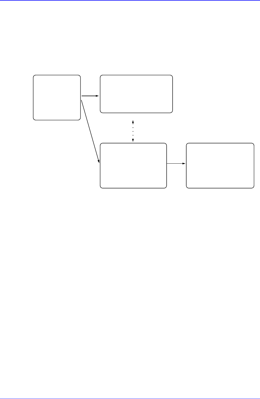
Whole Data
Register overall
information on
the component.
Lead Parameter
Data that have Lead
information on lead forms
Lead Group
Data that specify the
position where the lead
are converged.
Lead Gap
Information on the
position of empty in the
lead group
Figure 11-38. The basic concept of User IC component data setting
User IC component data has one whole data.
User IC component data has up to 16 lead groups.
User IC component data has equal or fewer lead parameters than the lead groups(up
to 8).
Each lead group must specify 1 corresponding lead parameter.
Each lead group has up to 4 lead gaps.
Samsung Component Placer CP-45F(V)/FS Operations Manual
11-60
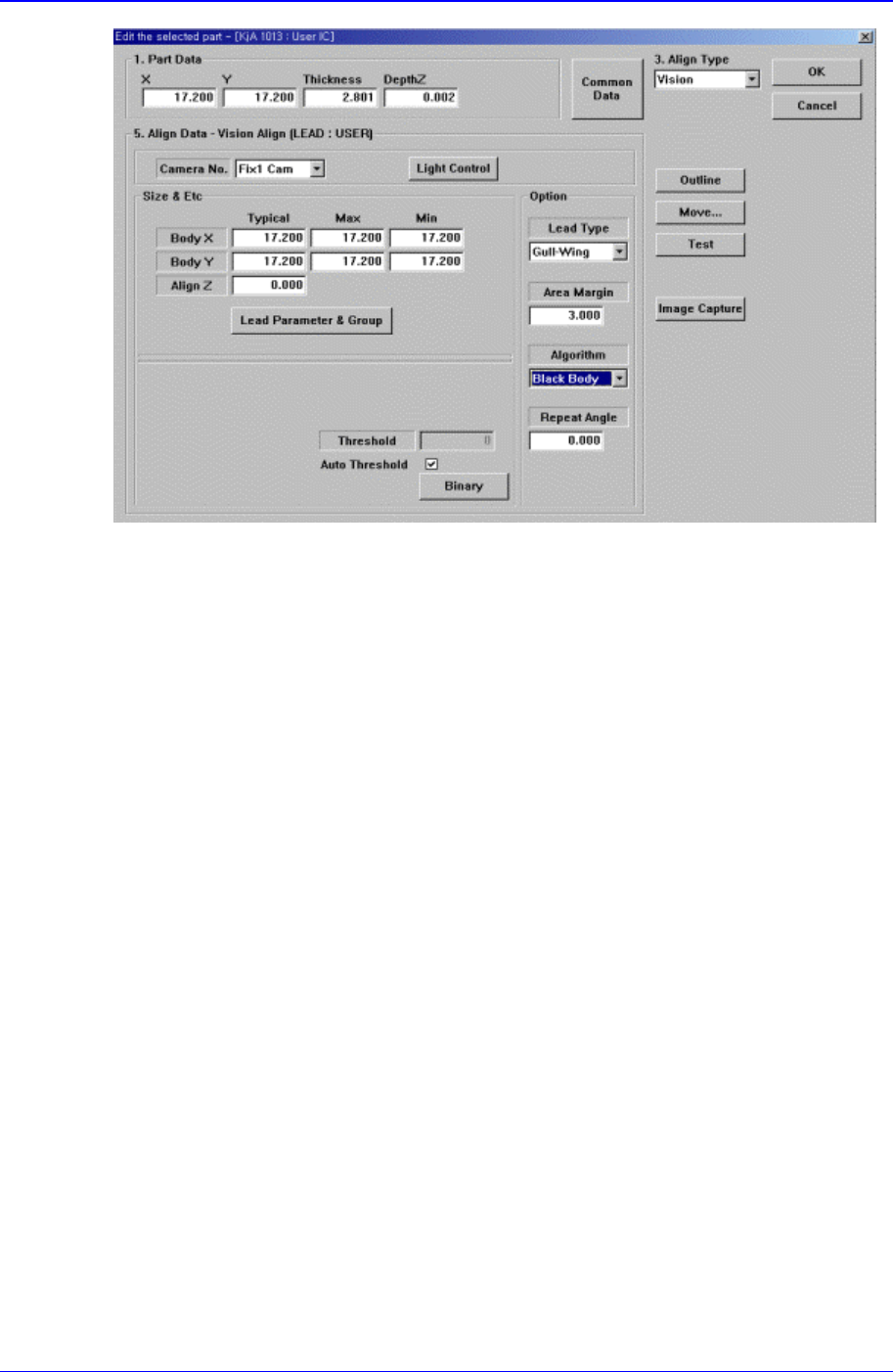
Figure 11-39. “Align Type = Vision, Package Group = User IC” dialog box
<Camera No.> combo box
Select the camera to recognize the component.
<Light Control> button
Set the light for the camera to recognize the component.
<Size & Etc> group
Set the align size.
<Body X Typical> edit box
Set the size of component body in X direction.
<Body X Max> edit box
Set the maximum size of component body in X direction.
<Body X Min> edit box
Set the minimum size of component body in X direction.
<Body Y Typical> edit box
Set the size of component body in Y direction.
<Body Y Max> edit box
Set the maximum size of component body in Y direction.
<Body Y Min> edit box
Set the minimum size of component body in Y direction.
<Align Z> edit box
Set the height for recognition. Based on the component surface, if the top is to be
recognized, set - value and if the bottom is to be recognized, set + value.
<Lead Parameter & Group> button
PCB Edit Command
11-61
Set the lead parameter and lead group. Please refer to <11.1.15.1 Lead
Parameter>, and <11.1.15.2 Lead Group>.
<Option> group
Set the align option data.
<Area Margin> edit box
Set the limit for the image to be off the center of the screen when the component
is recognized. For example, if this value is 5mm, then the image of the
component should be within 5mm of the center of the screen.
<Lead Type> combo box
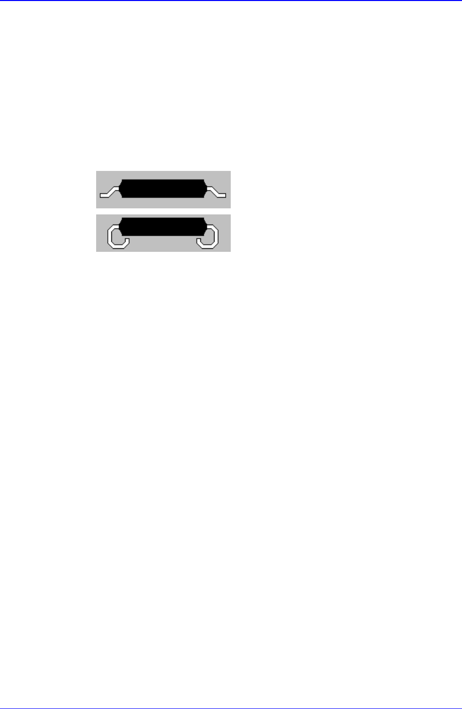
Select the lead type. Available lead types are as follows.
Gull-Wing: Leads protrude outward as QFP.
J-Lead: Leads roll inward as PLCC.
<Algorithm> combo box
Select the algorithm to recognize the component. Available algorithms are as
follows.
Black Body: Method to process IC types fast. In general, applied to IC types.
All Body: Applied to various types of components, but it takes long to process.
Applied to non IC types or hard to recognize components.
Odd with No Lead: Applied to odd type components without leads.
Odd with Lead: Applied to odd type components with leads.
When <Algorithm> is “Odd with No Lead” or “Odd with Lead”, the following
dialog box is displayed.