operation-cp45.pdf - 第176页
Samsung Component Placer CP-45F(V)/FS Operations Manual 11-22 Saves the bad mark data and closes the “ Bad Position ” dialog box. <Cancel> button Closes the “ Bad Position ” dialog box without saving the bad mark…
PCB Edit Command
11-21
<10. Parameter> group
<Threshold> edit box
Set the threshold value of <Bad Mark Logic> for bad mark inspection. For
example, if <Bad Mark Logic> is “Black” and the <Threshold> value is 100,
then all the values under 100 in the vision image are recognized as black, and
if <Bad Mark Logic> is “White” and the <Threshold> value is 100, then all
values over 100 are recognized as white.
<Light> group
Set the light value for bad mark inspection. In general it is 7, but adjust it
appropriately according to the condition of PCB and bad mark.
<Test> button
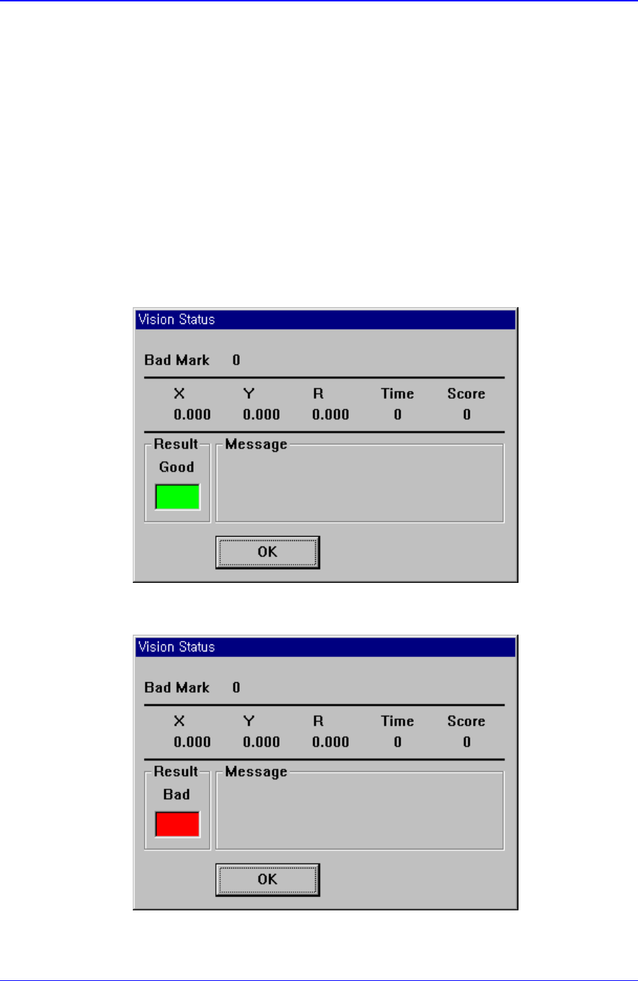
By using the registered mark information, tests the mark.. The accuracy of the
registered mark data can be verified. When the test is successful, the following
message box is displayed.
When the test is not successful, the following message box is displayed.
<OK> button
Samsung Component Placer CP-45F(V)/FS Operations Manual
11-22
Saves the bad mark data and closes the “Bad Position” dialog box.
<Cancel> button
Closes the “Bad Position” dialog box without saving the bad mark data.
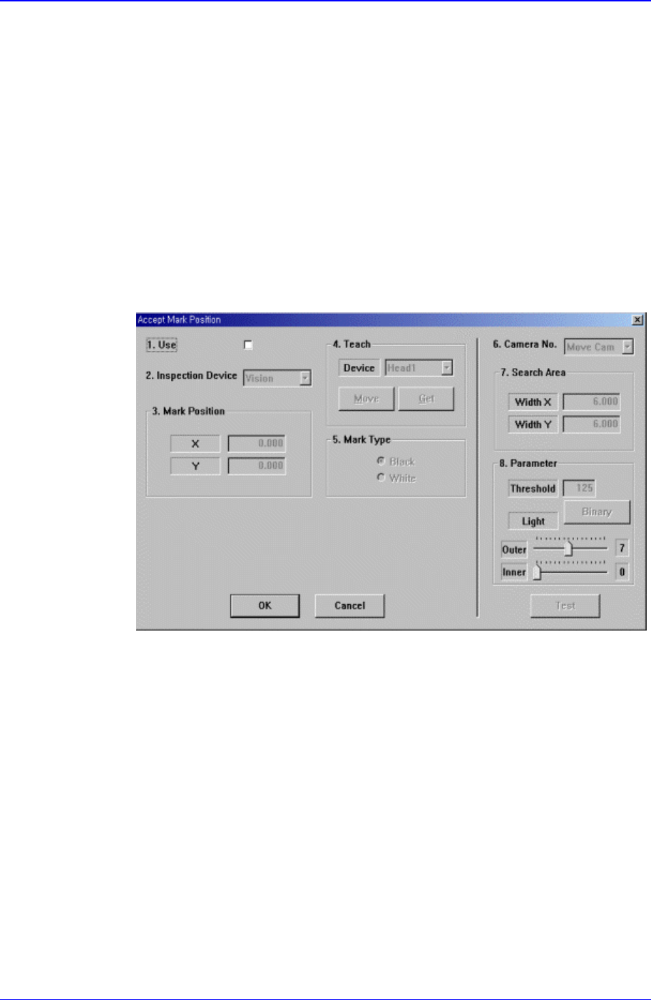
<Accept Mark…> button
A bad mark is a mark that indicates whether a loaded PCB is good or defective.
When a PCB is defective, the bad mark is marked but the accept mark is not marked,
and only the marked PCBs are worked on. When this button is clicked on, the
following dialog box for the editing of accept mark data is displayed.
<1.Use> check box
Use it to select or check the use of Accept Mark.
<2. Inspection Device> combo box
Select the device to test the Accept Mark. Available device is as follows.
Vision: Recognizes with the move camera in the Head Block.
Figure 11-16. “Accept Mark Position” dialog box (Checked in ‘Use” check box)
<3. Mark Position> group
Shows the position of Accept Mark.
<4. Teach> button
Teaches the accept mark offset value with the method same as the one used to
teach the PCB size.
<5. Logic> group
Select the color of Accept Mark. Available mad mark colors are as follows.
Black: the mark appears darker than the surrounding.
White: the mark appears brighter than the surrounding.
<6. Camera No.> combo box
Select the camera to test the Bad Mark. At present, it is fixed to “Move Camera”.
<7. Search Area> group

PCB Edit Command
11-23
Set the area to test the Accept Mark. The purpose is to limit the testing area when
recognition is interfered due to a shape similar to the mark near the mark.
<Width X> edit box
Set the range to test in X axis direction. In general, set to 6mm.
<Width Y> edit box
Set the range to test in Y axis direction. In general, set to 6mm.
<8. Parameter> group
<Threshold> edit box
Set the threshold value of <Bad Mark Logic> when testing the Accept Mark.
For example, if <Accept Mark Logic> is “Black” and the <Threshold> value
is 100, all values under 100 in the vision image are recognized as black. And
if <Accept mark Logic> is “White” and the <Threshold> value is 100, all
values over 100 in the vision image are recognized as white. On the vision
display, the image for which the threshold value is applied is in the binary
mode and the image for which the threshold value is not applied is the real
display.
<Light> group
Set the lighting value when testing the Accept Mark. In general, set to 7.
However, adjust it properly according to the condition of the PCB and accept
mark.
<Test> button
Tests the mark by using the set mark data. The user can check whether the set
mark data is correct.
<PCB In> button
Loads the PCB in the operation area.. Before executing this function, the PCB
arrangement method must be set in “Fix Type” of <7. Handling>.
<PCB Out> button
Releases the PCB fixed in the operation area.
<Stopper U/D> button
Moves up or down the work stopper, the stopper of PCB in the operation area.
<BUT U/D> button
Moves up or down the BUT(Back Up Table) that locks up the PCB in the operation
area.
<Cancel> button
Cancels the edited data.
Caution - If you move to another screen while editing the “Board” dialog box, the
edited data is saved automatically.
11.1. Part [F3]
The <Part> command is used to register components necessary for PCB operation and
edit data.
The component data managed by this equipment include PCB Part, Local Part Library,
and Standard Part DB. The following is the structure of each data and the relationship