operation-cp45.pdf - 第172页
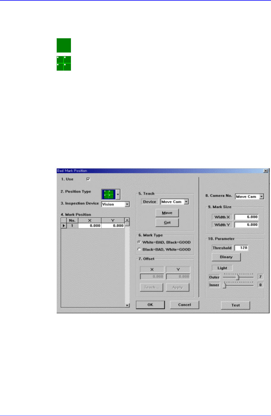
Samsung Component Placer CP-45F(V)/FS Operations Manual 11-18 Use it to select or check the use of bad mark. <2. Position T y pe> combo box Select the position of bad mark. Available positions of bad marks are as…
PCB Edit Command
11-17
When the test is not successful, the following message box is displayed.
<Repeat…> button
It is not explained here as it is displayed in the debug mode only.
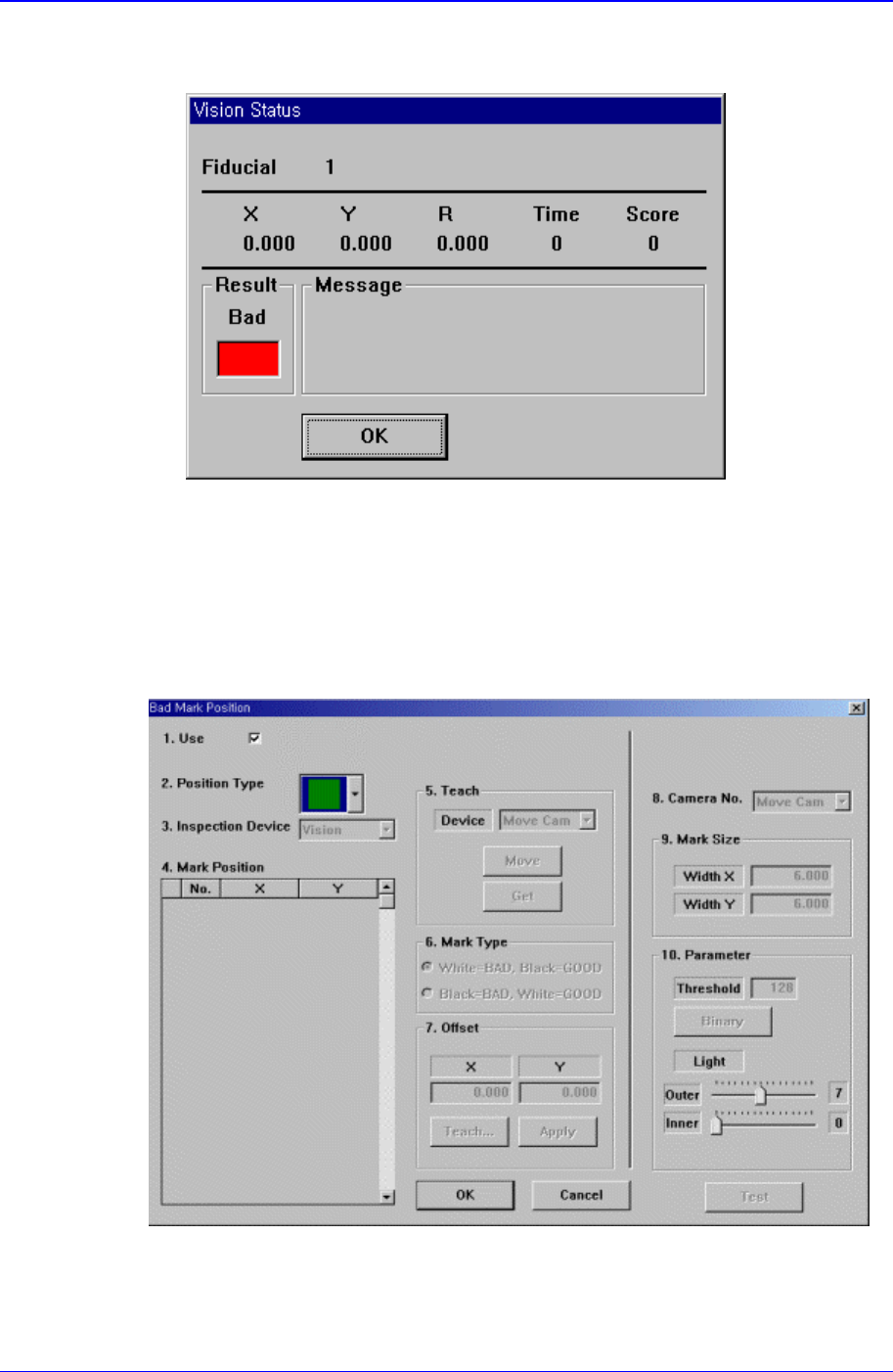
<Bad Mark…> button
A bad mark is a mark that identifies whether the loaded PCB is good or bad. The
PCB marked as bad is not operated. When this button is clicked on, the following
dialog box to edit bad mark data is displayed.
Figure 11-14. “Bad Mark Position” dialog box(When the Position Type is “None”)
<1.Use> check box
Samsung Component Placer CP-45F(V)/FS Operations Manual
11-18
Use it to select or check the use of bad mark.
<2. Position Type> combo box
Select the position of bad mark. Available positions of bad marks are as follows.
None: No bad mark.
Array: 1 bad mark in each array PCB.
<3. Inspection Device> combo box
Select the device for bad mark inspection. Available devices are as follows.
Vision: Recognizes with the move camera in the head block.
<4. Mark Position> group
When <Position Type> is not “None”, data is generated according to the selected
<Position Type>. The number of data generated is as follows.
When the <Position Type> is “Array”: 1
When the <Position Type> is “Panel”: The number of Array PCBs
For example, when “Array” is selected in <Position Type>, the following dialog
box is displayed. (When the number of Array PCBs is 4)
Figure 11-15. “Bad Mark Position” dialog box(When the Position Type is “Panel”)
<No> column
A serial number of bad mark data.
<X> column
The X position value of the bad mark.
<Y> column
The Y position value of the bad mark.
<5. Teach> group
Used to move the XY axis of the equipment to the specified position or to read in
PCB Edit Command
11-19
the current position of the XY axis.
<Device> combo box
To move or to read in the position of the XY axis, select the corresponding
device. Available devices are as follows.
Move Cam: Selects the teaching camera.
Head1: Selects Head1.
Head2: Selects Head2.
Head3: Selects Head3.
Head4: Selects Head4.
Head5: Selects Head5.
Head6: Selects Head6.
<Move> button
Moves the XY axis to the device selected in <Device>. Before executing
“Move, the cell in the grid corresponding to the desired position must be
clicked on with a mouse.
<Get> button
Reads in the current position of the XY axis of the device selected in
<Device>. Before executing, “Get”, the cell in the grid corresponding to the
desired position must be clicked on with a mouse.
<6. Logic> group
Select the color of bad mark. Available colors of bad marks are as follows.
Black: the mark looks darker than the surroundings.
White: the mark looks lighter than the surroundings.
<7. Offset> group
Used to set the offset value between bad marks automatically.
<X> edit box
Set the offset value of X.
<Y> edit box
Set the offset value of Y.
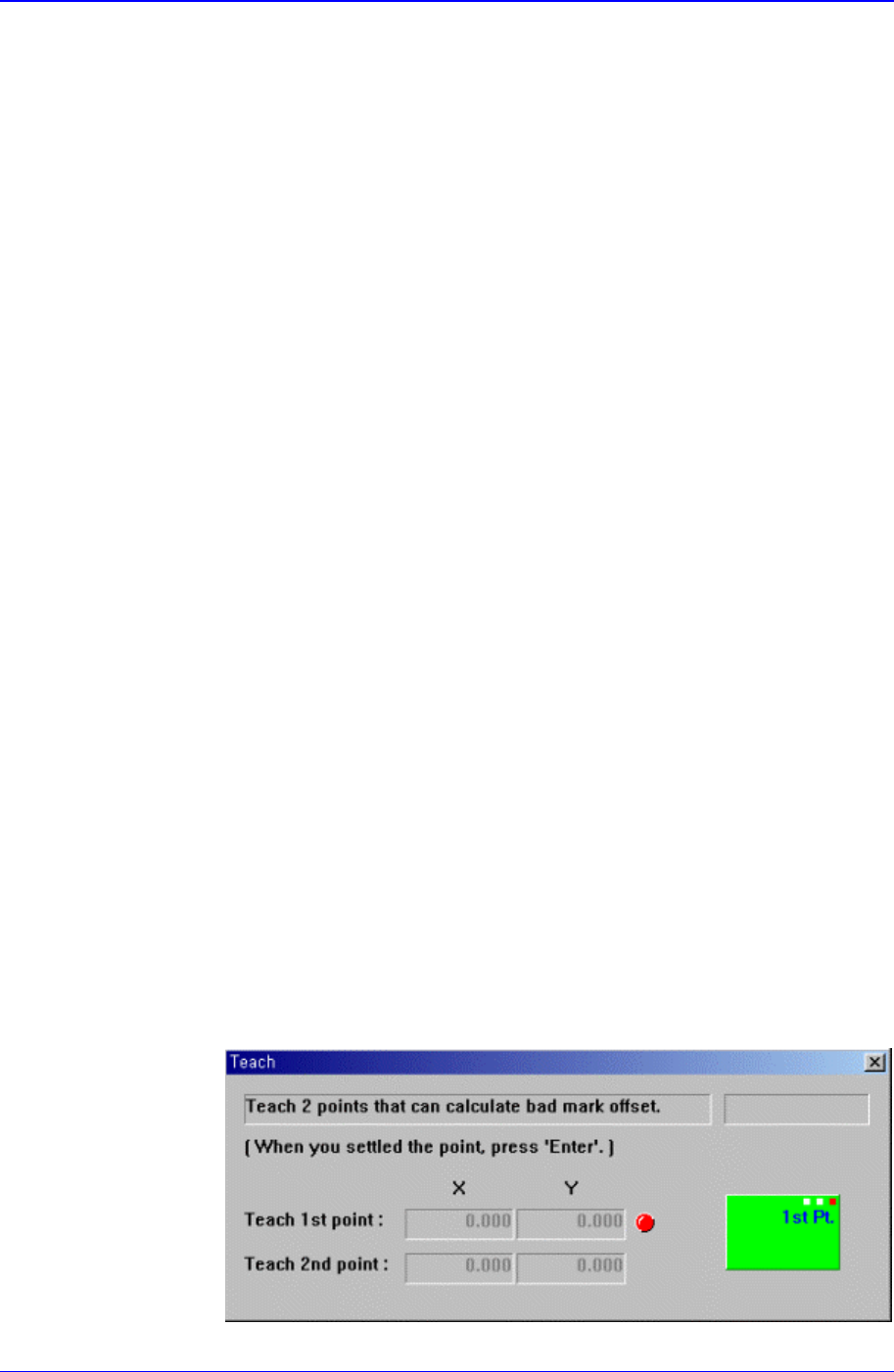
<Teach> button
Teach the offset value of bad mark by using the same method as teaching the
PCB size. When this button is clicked on, the following screens are displayed
in succession.