operation-cp45.pdf - 第170页
Samsung Component Placer CP-45F(V)/FS Operations Manual 11-16 By using the registered mark information, finds the exact size of the mark. After the size of the actual mark is found, the following message box is displa ye…

PCB Edit Command
11-15
180: the mark is rotated to 180°.
270: the mark is rotated to 270°.
<7. Search Area> group
Set the area in which to search the fiducial mark. The main purpose of this
feature is to limit the search range for when there are forms similar to the mark
near the mark such that they can interfere with recognition on certain PCBs.
<X> edit box
Set the position to start searching for the fiducial mark in X axis. The center
of the vision monitor screen is 0. In general, it is -3 mm.
<Y> edit box
Set the position to start searching for the fiducial mark in Y axis. The center
of the vision monitor is 0. In general, it is -3 mm.
<Width X> edit box
Set the value of search range in X axis. In general, it is 6 mm.
<Width Y> edit box
Set the value of search range in Y axis. In general, it is 6 mm.
<8. Parameter> group
<Score> edit box
The accuracy with which the fiducial mark matches the given data expressed
in number is “score”. The score ranges from 0 to 100. The value set in
<Score> denotes the minimum “score” to be accepted. In general, it should be
at least 600(default value) for accurate adjustment. Even in the worst case, it
should be over 300.
<Light> group
Set the light value when the fiducial mark is inspected. In general, 7 is
appropriate but it can be adjusted according to the condition of PCB and
fiducial mark.
<Tuning> button
Samsung Component Placer CP-45F(V)/FS Operations Manual
11-16
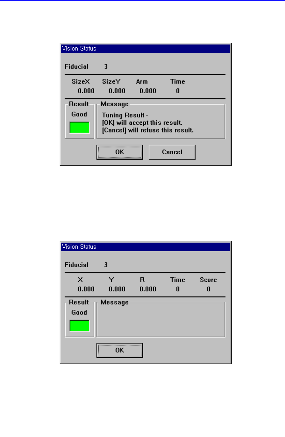
By using the registered mark information, finds the exact size of the mark. After
the size of the actual mark is found, the following message box is displayed. If
you want to update it with the data found, click on the<Yes> button, otherwise
click on the <No> button.
<Outline> button
Displays the shape of the mark on the vision monitor screen by referring to the
registered mark data. This feature is used to check whether the registered value
coincides with the actual mark.
<Test> button
By using the registered mark information, tests the mark.. The accuracy of the
registered mark data can be verified. When the test is successful, the following
message box is displayed.
PCB Edit Command
11-17
When the test is not successful, the following message box is displayed.
<Repeat…> button
It is not explained here as it is displayed in the debug mode only.
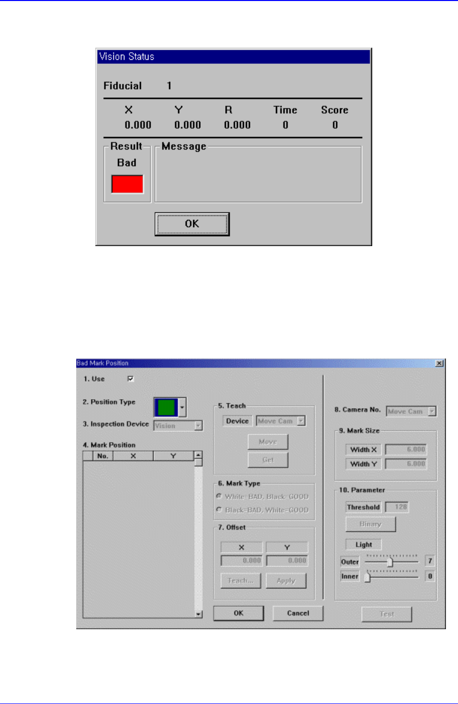
<Bad Mark…> button
A bad mark is a mark that identifies whether the loaded PCB is good or bad. The
PCB marked as bad is not operated. When this button is clicked on, the following
dialog box to edit bad mark data is displayed.
Figure 11-14. “Bad Mark Position” dialog box(When the Position Type is “None”)
<1.Use> check box