operation-cp45.pdf - 第66页
Samsung Component Placer CP-45F(V)/FS Operations Manual 2-14 2.8. Detection of Impr oper Component Pickups A vacuum sensor that can detect improper adsorption of components due to fluctuations in the vacuum pressure duri…
Basic Configuration and Name of Each Part
2-13
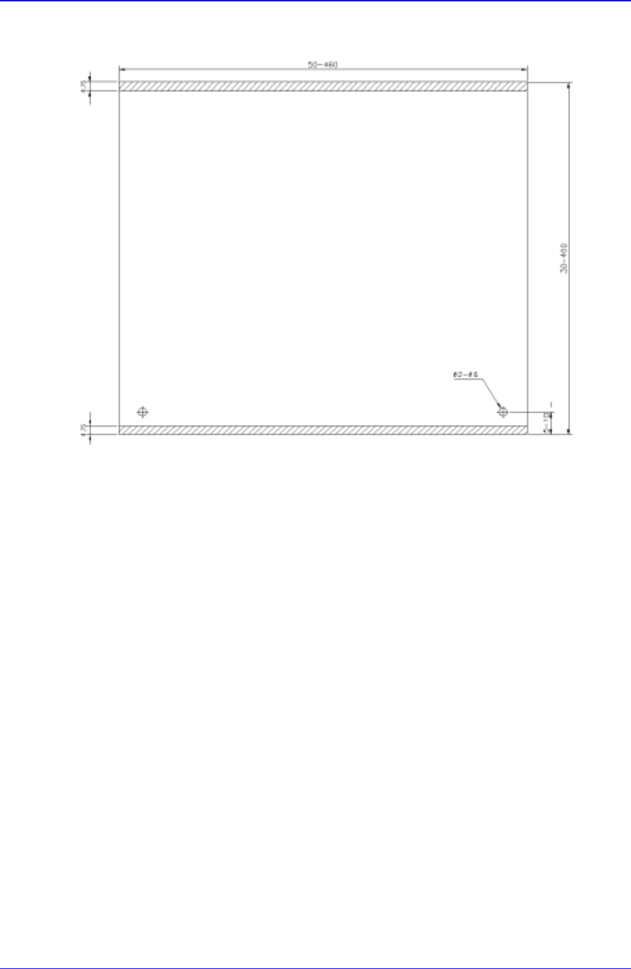
2.7.5. Conditions for PCB
Figure 2-9. Conditions for PCB Limit
There is a 4.75mm extra spacing at the edge of the board. The upper margin is 17mm,
while the lower margin is 14.5mm. The board is supported by using a back-up pin with
135mm height.
PCB fixing method
The CP-45F/V and CP-45FS fixes PCB's with a position-fixing pin. Another method
of fixing the side of PCB's can also be selected, and a combination of the above two
methods is possible.
The present specifications should be adjusted at the time of delivery.
PCB transport direction and the position of a position-fixing pin
It is possible to transfer PCB from left to right or vice versa. It is desirable that the
user request for our assistance for switching the transport direction.
The position of a fixing pin can be arbitrarily designated by the user. The PCB
transport direction and the position of a fixing pin can be set as desired by the user at
the time of delivery.
Samsung Component Placer CP-45F(V)/FS Operations Manual
2-14
2.8. Detection of Improper Component Pickups
A vacuum sensor that can detect improper adsorption of components due to fluctuations
in the vacuum pressure during adsorption is provided. A default vacuum pressure values
during adsorption is set for each nozzle, and it also can be set as desired for each nozzle
for safe adsorption.
In the vision recognition mode, vacuum sensor will only detect improper adsorption of
components.
2.9. PCB Coordinate Correction Function (Fiducial Mark Recognition)
This function is to correct the placement position by comparing the position of the
fiducial mark that has already been inputted with the read-in position of the fiducial mark
indicated on PCB by using a move camera.
There are two methods of correction: one is a global correction, the other is a local
correction.
Global correction
Each point is corrected based on one or two points in a PCB. In the case of an array
PCB, correction can be made for each arrayed PCB.
Local correction
Fiducial correction is made for each important point (QFP, etc.) in a PCB.
Corrections can be selectively made on the components requires the corrections.
The correction of fiducial mark recognition coordinate is possible only if a mark that
can serve as a reference on the PCB exists.
Performing a local correction of each component after a global correction of each
PCB allows high-precision placement of the component by ensuring more reliable
correction of the component position.
Fiducial mark recognition is rather limited for our CP-45FV model. please contact
our Business Department or C/S Center.
Memo

Basic Configuration and Name of Each Part
2-15
2.9.1. Fiducial inspection
2.9.1.1. Types of fiducial mark
Figure 2-10. Types of Fiducial Mark
Repeatability: ± 5㎛
Resolution: 43 ㎛/pixel ± 5%
Image processing speed: 100 msec (ø 2mm circle )
2.9.1.2. Size and allowable tolerance of fiducial mark
The outer size of each fiducial mark is 0.5 mm - 5.0 mm, and the allowable tolerance
should be within 10%.
2.9.1.3. Clearance area
Each fiducial mark should have a square clearance area, around which there is no other
marks such as a conductor patterns, remaining leads, markings, etc. The square clearance
area should secure at least 0.5mm from the outer edge of the circumference of the mark.
In other words, there should be no mark within 0.5mm from the boundary of the fiducial
mark.
2.9.1.4. Basic materials and surface treatment of marks
All recognition marks should be coated with non-surface-treated copper clad or one of the
following materials.
Transparent non-oxidizing coating.
Nickel coating
Tin coating