operation-cp45.pdf - 第68页
Samsung Component Placer CP-45F(V)/FS Operations Manual 2-16 Lead plating Gold plating Hot-wing repeller solder coating Flux coating The surface of a fiducial mark should appear in complete contrast to printed ci…

Basic Configuration and Name of Each Part
2-15
2.9.1. Fiducial inspection
2.9.1.1. Types of fiducial mark
Figure 2-10. Types of Fiducial Mark
Repeatability: ± 5㎛
Resolution: 43 ㎛/pixel ± 5%
Image processing speed: 100 msec (ø 2mm circle )
2.9.1.2. Size and allowable tolerance of fiducial mark
The outer size of each fiducial mark is 0.5 mm - 5.0 mm, and the allowable tolerance
should be within 10%.
2.9.1.3. Clearance area
Each fiducial mark should have a square clearance area, around which there is no other
marks such as a conductor patterns, remaining leads, markings, etc. The square clearance
area should secure at least 0.5mm from the outer edge of the circumference of the mark.
In other words, there should be no mark within 0.5mm from the boundary of the fiducial
mark.
2.9.1.4. Basic materials and surface treatment of marks
All recognition marks should be coated with non-surface-treated copper clad or one of the
following materials.
Transparent non-oxidizing coating.
Nickel coating
Tin coating
Samsung Component Placer CP-45F(V)/FS Operations Manual
2-16
Lead plating
Gold plating
Hot-wing repeller solder coating
Flux coating
The surface of a fiducial mark should appear in complete contrast to printed circuit part
so that it is clearly distinguishable from the circuits that are already printed. It should
always be clean without dirt or contamination.
2.9.1.5. Evenness of fiducial marks
The surface of a fiducial mark should be even and smooth. Unevenness of the surface
should be within 0.02mm, and a material covering the surface of a fiducial mark should
also be even and smooth (That is, the protruding portion from the fiducial mark surface
should be within 0.02mm.).
2.9.1.6. Bad-Marks
If you don't want a component to be placed on a PCB, indicate the bad-mark on the PCB
(The position of bad-mark should be consistent).
It should appear in complete contrast to the background color of PCB, and have a
diameter of more than 2.5mm.
In the production program, a shading(dark or light) indication with respect to the
background color of PCB may be designated arbitrarily as a bad-mark.
Warning
Pressing the Start switch without checking the presence
of worker nearby could cause injury.
Be sure to check if there is any worker near the machine
before pressing the Start switch.
Memo
Basic Configuration and Name of Each Part
2-17
2.10. Component Alignment Method (Component Centering Method)
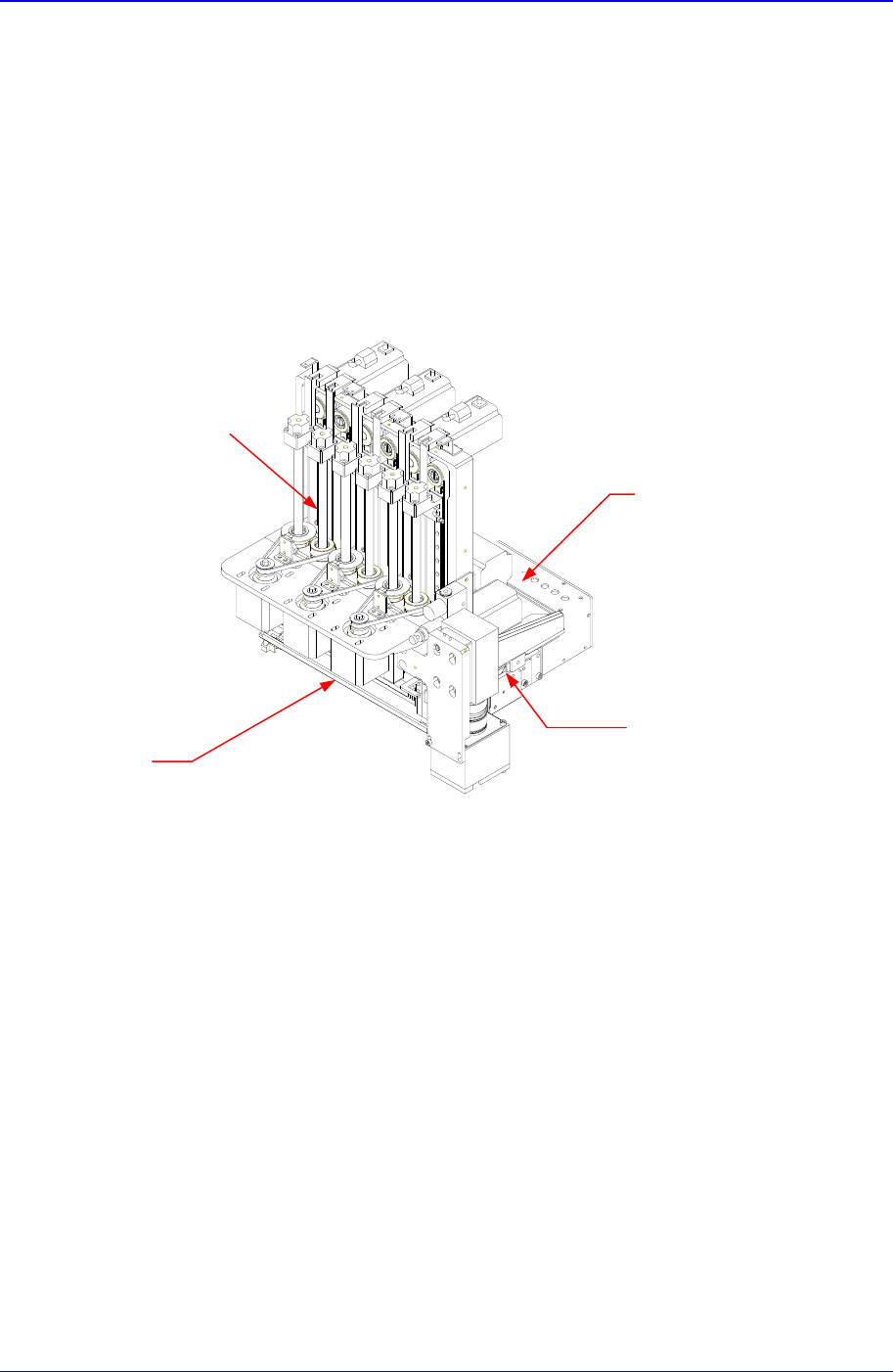
2.10.1. Flying Vision
2.10.1.1. Overview
The flying vision system is a vision system attached on the head that recognizes a
component when it moves from the pickups position to the placement position. 6 CCD
cameras attached on the head recognize components on 6 heads simultaneously. 3 types
of multiple step digital lights can be selected for each head.
Figure 2-11. Samsung Flying Vision
2.10.1.2. Light Path Control
The flying vision system has a mirror on the light path. To avoid a collision with the Z
axis, it rotates during pickups, recognition, and placement.
6-CCD Camera
Multi-Step digital
lighting system
Mirror
6-Head