YV180X_Ope_E.pdf - 第161页
5 -85 EPD8013110 Operation Chapter 5 5 Creating the PCB data 5. Run the P ARAM SEARCH command again and, if successful, next run the VISION TEST command. When no error occurs, advance to the next step. If the P ARAM SEAR…
5
-84
EPD8013110
Operation
Chapter 5
5
Creating the PCB data
5 Run the VISION TEST command.
Repeat this test several times. When no errors occur, the parameter settings
are appropriate. Advance to the next step. If an error occurs, adjust the
parameters with the procedure below.
1. Return to the Mark Info. screen with the EXIT command, and check that
the following parameters are set correctly.
Mark Type and MarkOutSize in the Mark Type Info. sub-
window
Shape Type and Surface Type in the Vision Info. sub-window
2. After checking the parameters, press the [F6] key to open the Adjust
Assistant screen again, then repeat Steps 4 to 5.
When no errors occur, move to the next step.
3. If an error still occurs, run the PARAM SEARCH command to find an
optimum threshold level.
4. After the optimum threshold level has been found, run “VISION TEST”
again.
When no errors occur, go to the next step.
If the optimum threshold level could not be obtained, run the CHK
THRESHOLD command.
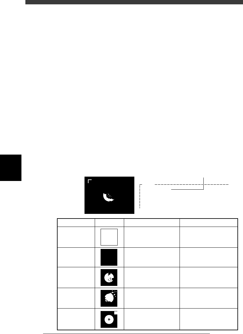
A binary image will be displayed on the vision monitor according to
the current parameter settings as shown below. Adjust the threshold
level as suggested below, so that the mark image is clearly displayed.
Binary image (mark)
23534-C0-00
V192
(LEVEL=150)
Binary image is on the monitor......
[INS] or [DEL] key to change the threshold.
Hit [ENTER] to finish.
Current threshold setting
State
All white
All black
Noise within
mark
Noise outside
of mark
Other than
mark in
search area
Image Countermeasure
Increase the Mark
Threshold level with the
[INS] key.
Decrease the Mark
Threshold level with the
[DEL] key.
Increase the Cut Inner
Noise level in the Adjust
Assistant.
Increase the Cut Outer
Noise level in the Vision
Info. sub-window.
Decrease the Search
Area level in the Vision
Info. sub-window.
Remarks
Adjust it till the mark is
displayed.
Adjust it till the mark is
displayed.
Refer to "Search Area"
explained previously.
Recognition time becomes
longer as the Cut Inner
Noise level is increased.
Recognition time becomes
longer as the Cut Outer
Noise level is increased.
5
-85
EPD8013110
Operation
Chapter 5
5
Creating the PCB data
5. Run the PARAM SEARCH command again and, if successful, next run
the VISION TEST command.
When no error occurs, advance to the next step.
If the PARAM SEARCH result is a fail, enter a larger value for the
Tolerance parameter in the Adjust Assist Items window, then run
“PARAM SEARCH” again.
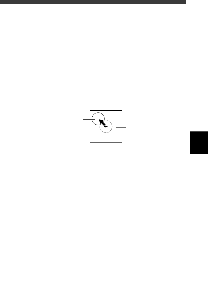
6 Check that the mark can be recognized even if it has
moved.
Check that the mark can be recognized in any location within the search
area.
Run the TEACH MARK command, and manipulate the joy stick to move
the mark slightly. If no error occurs when “VISION TEST” is run again, the
setting is okay. Repeat this operation several times, and check that no error
occurs.
Final check (mark)
23535-C0-00
Check that the mark is correctly recognized
even when slightly shifted from the center cursor
Search Are
a
7 Select the EXIT command.
Now you can exit the Adjust Assistant mode and return to the Mark
Info. screen.
5
-86
EPD8013110
Operation
Chapter 5
5
Creating the PCB data
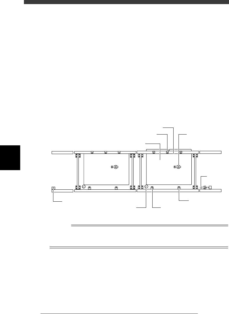
5. Clamping the PCB
When you clamp a PCB on the conveyor manually, for example when
teaching the coordinate data on the PCB, set it on the conveyor with the
procedure below.
There are three methods of clamping a PCB. Select the method that
matches the PCB to be used.
1. “Locate Pin”
2. “Pin+PushUp”
3. “Edge Clamp” (option)
Methods 1 and 2 use the locate pins for PCB positioning but method 3 does-
not use locate pins. Refer to “8. Changing the conveyor unit setup” in
Chapter 4 for adjustment of each conveyor unit.
Conveyor unit (top view)
23536-D8-00
Edge clamp (option)
PCB clamp
Push-up plate
Push-up pin
Main stopper
A-table conveyor
B-table conveyor
Fixed locate pin
Movable locate pin
Entrance
stopper
Exit stopper
Reference
The PCB clamping method can be selected by specifying the PcbFixDevice parameter on
the PCB Info. screen. For details on the PCB clamping method, refer to Step 12 of “6.
Creating the PCB information” in this chapter.