YV180X_Ope_E.pdf - 第180页
5 -104 EPD8013110 Operation Chapter 5 5 Creating the PCB data Refer ence T o perform teaching at a mounting position, set the teaching conditions as follows. TEA CH-T ABLE SEL. (T eaching table) : Select the A or B table…
5
-103
EPD8013110
Operation
Chapter 5
5
Creating the PCB data
4 Enter the XY data.
For single PCBs, enter the XY coordinate data of the center of the mount-
ing position relative to the PCB origin (see “6.2” in this chapter). In the
case of multi-block PCBs, enter the position data relative to the block
repeat No.1 (see Chapter 6).
You can also use the teaching function to enter the XY coordinate data as
explained below.
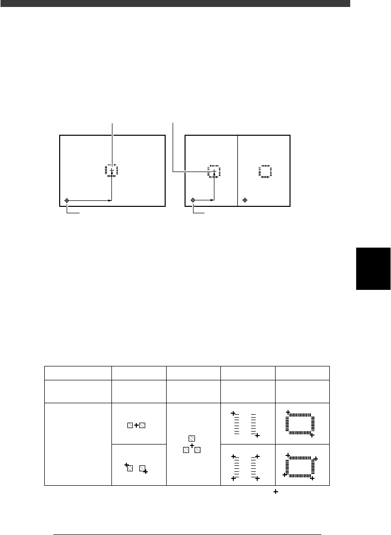
Mounting position relative to the PCB origin
23548-C0-00
Block 1 Block 2
Center of mounting position
PCB origin Block repeat No.1
To perform teaching to enter the XY coordinate data, proceed as follows:
1. Move the cursor to the “X” or “Y” column on the Mount Info. screen.
2. Manipulate the joystick to move the teaching camera so that the cross
cursor on the vision monitor is aligned with the teaching position.
For single point input, press the [F10] key twice.
For multi-point inputs, press the [SHIFT]+[F10] keys twice at the first
point and once at the second and third points, then press the [F10] key
only at the final point.
Typical teaching methods are shown in the table below. Use any desired
teaching method.
Teaching method for each component
25516-C0-00
Component type
Teaching method
Teaching point
CHIP Tr. SOP
QFP
: Teaching point
1 or 2-point
input
1-point
input
2 or 4-point
input
2 or 4-point
input
5
-104
EPD8013110
Operation
Chapter 5
5
Creating the PCB data
Reference
To perform teaching at a mounting position, set the teaching conditions as follows.
TEACH-TABLE SEL. (Teaching table): Select the A or B table head you will use.
TEACH-UNIT SEL. (Teaching unit) : Camera
SPEED SELECT (Axis moving speed) : 10 to 20
FIDUCIAL SEL (Fiducial correction) : Use (Select “NotUse” if not using
a fiducial mark.)
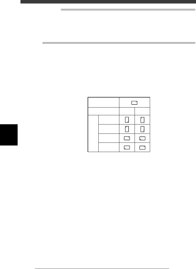
5 Enter the mounting angle in the “R” column.
Enter the angle through which the component must be rotated after
recognition before it is mounted on the PCB. When the pickup angle (in
the PICK AND MOUNT INFO. sub-window of the Component Info.) is 0°,
enter the rotating angle from the loading position, with the counterclock-
wise direction specified as a plus value when viewed from above. When
the pickup angle is 90° or -90°, see the table below.
Mounting angle
25517-C0-00
Loading position
Pickup angle
90 deg. -90 deg.
0 deg.
180 deg.
90 deg.
-90 deg.
Mounting angle
6 Check the head number in the “Head” column.
The head number to be used for mounting is indicated in the “Head”
column. Since the optimum head number is automatically selected when
you run the DATA_GENERATOR command described later, it is not
necessary to enter it here. (Refer to “9. Data optimization” in this chapter
for details.)
If you do not use the DATA_GENERATOR command, enter the head
number you will use for component mounting.
7 Set the fiducial mark number in the “FidMk” column.
Enter the number of the fiducial mark (point, local or 4-point fiducial) to
be used for this mount data. (Refer to “5.2 Local fiducial function” in
Chapter 6.) Note that this setting is valid only when necessary data is input
in the Local Fidu. Info. Enter “0” when not using the fiducial function.
8 Set the badmark number in the “BadMk” column.
Enter the number of the local badmark to be used for this mount data.
(Refer to “6.2 Local badmark” in Chapter 6.) Note that this setting is valid
only when necessary data is input in the LocalBadMrkInfo. Enter “0” when
not using the local badmark function.

5
-105
EPD8013110
Operation
Chapter 5
5
Creating the PCB data
9 Set the “Skip?” column.
Select “Exec.” to use this mount data, and select “Skip” when not using it.
n
NOTE
If block conversion in <2/2/DATA_GENERATOR> runs on the multi-block PCB data (to
convert multi-block PCB data into single PCB data), the “Exec” settings in the original
data will be saved as “NOTE DATA”.
0 Save the data.
After setting all mount data, press the [ESC] key twice to exit the current
edit screen, then select <2/1/D8 SAVE PCB DATA> and press the [ENTER]
key.