YV180X_Ope_E.pdf - 第85页
5 -9 EPD8013110 Operation Chapter 5 5 Creating the PCB data 3 Select the item you want to edit or create. After you have selected the PCB name, the edit menu appears, so select the item you want to edit or create. The se…
5
-8
EPD8013110
Operation
Chapter 5
5
Creating the PCB data
2.2 Selecting the PCB name
To edit the PCB data you already registered, you must first select the PCB
name.
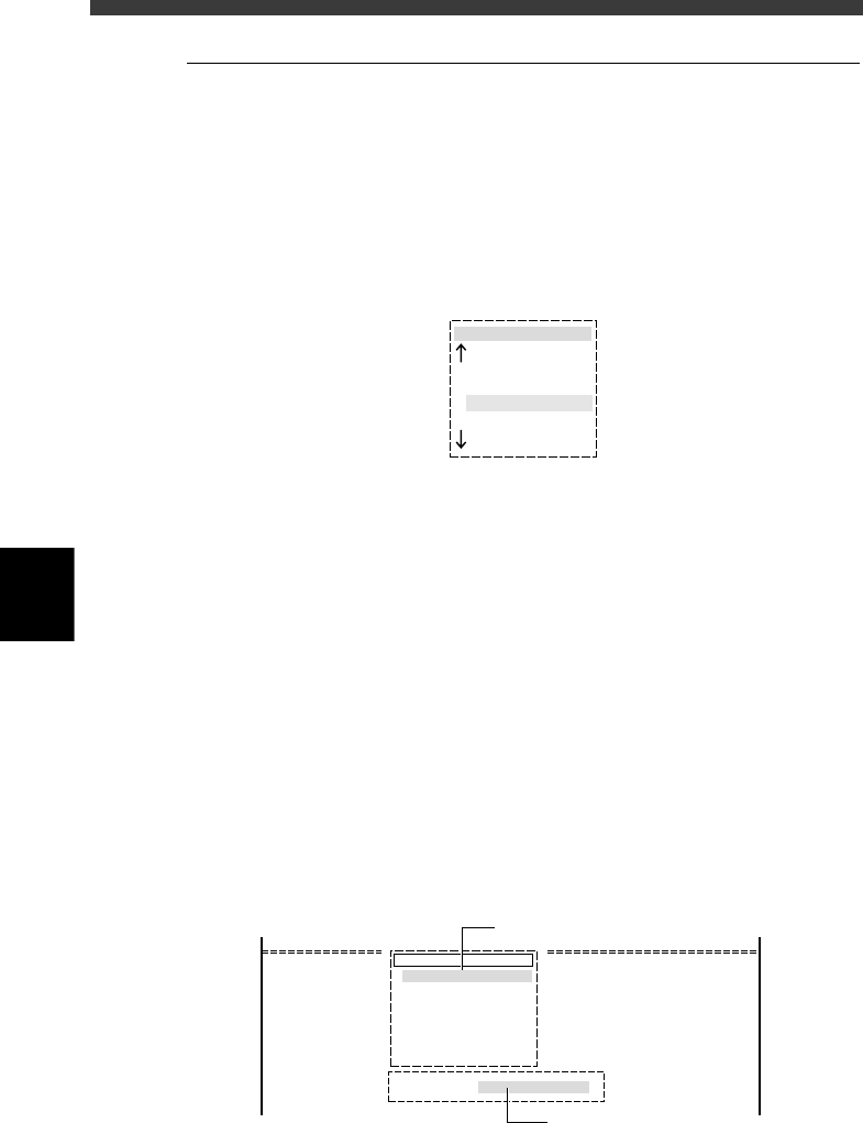
1 Run the <2/1/D1 SWITCH PCB DATA> command.
The “pcb name” selection box then appears showing a list of registered
PCB names.
When you are already in the EDIT_DATA mode, pressing the [F2] key
displays the “pcb name” selection box.
PCB name selection box
27503-C0-00
pcb name
CONVEYOR
ANC_TEST
CUK_100
PCB1
2 Select the PCB name.
There are the following two methods for selecting the PCB name.
1. Using the arrow keys (or PageUp/PageDown keys)
Using the up/down arrow keys (or PageUp/PageDown keys), move the
cursor to the PCB name for which you will edit data, and press the
[ENTER] key.
2. Typing the PCB name
On the screen showing the PCB name selection box, you can select the
PCB name by typing its first few letters from the keyboard, in the
Search PCB box which appears upon typing the first letter of the PCB
name. At the same time, the cursor in the PCB name selection box
moves to a PCB name that matches the letters you typed. (This method
will prove convenient when many PCB names are already registered.)
When the target PCB is selected, press the [ENTER] key. To change the
PCB name you have just typed, press the [Back Space] key to delete the
last letter one by one and retype the correct letters.
Search PCB box
27504-C0-00
pcb name
CUK_92001_1
TCO1M2
TCO1M1
TCO1M1_P
Search PCB : CUK
Type the PCB name here.
Cursor moves as you type the PCB name
in the Search PCB box.
5
-9
EPD8013110
Operation
Chapter 5
5
Creating the PCB data
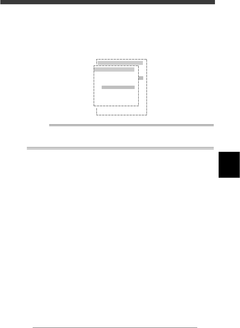
3 Select the item you want to edit or create.
After you have selected the PCB name, the edit menu appears, so select
the item you want to edit or create.
The selected information screen then appears. The PCB name is displayed
on the top of the screen (DATA [ ] column).
Selecting the edit item
27505-C0-00
pcb name
CONVEYOR
ANC_TEST
PALLET_88
PCB1
OBJECT
PCB Info.
Mount Info.
Component
Mark
Blk Repeat
Local Fidu.
LocalBadMrkI
Info.
Info.
Info.
Info.
Info.
n
NOTE
To switch the PCB data on the edit screen, press the [F2] key (or select <2/1/D1 SWITCH
PCB DATA>) . To switch the edit item, press the [F3] key (or select <2/1/A1 MAIN
WINDOW>).
5
-10
EPD8008100
Operation
Chapter 5
5
Creating the PCB data
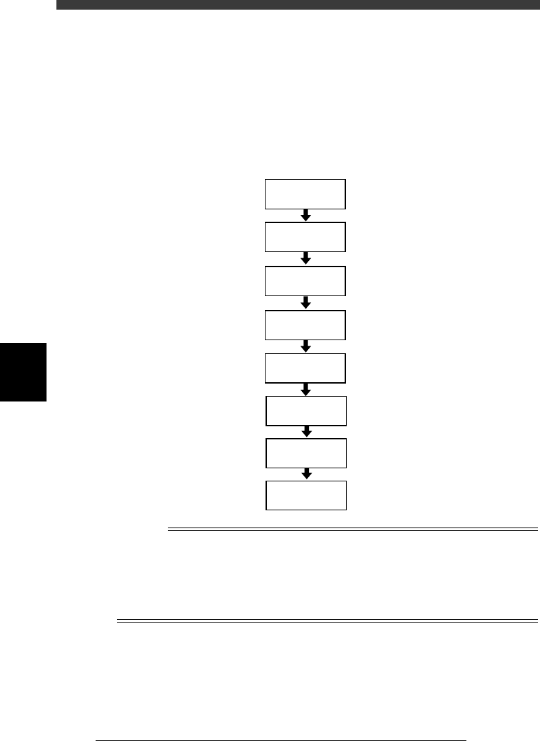
3. Creating the component information
The flow chart below shows the procedure for creating data on components
to be mounted on a PCB. Component data has various parameters for each
of the component names registered. To set these parameters, it is conve-
nient to copy sample data of a component with a similar shape from the
database (<2/3 DATABASE>) and then edit only the different parameters.
Flow chart for creating component data
23505-C0-00
Save data
Execute Adjust
Assistant
3.7
☞
Set various
parameters
3.2
☞
Enter feeder
set No.
Copy information
from database
Enter comment
Enter component
name
Open
component info.
Reference
In <2/3/DATABASE>, various kinds of component data are pre-registered as the YAMAHA
database. You can also create the user database for your own purpose. (See “3. Creating
the user database” in Chapter 6.)
To create PCB data more efficiently, it is advisable to register the component data in the
appropriate location by considering how the component is to be used. Refer to “3.9
Registration location of component data” in this chapter for more details.