YV180X_Ope_E.pdf - 第178页
5 -102 EPD8013110 Operation Chapter 5 5 Creating the PCB data 1 Open the Mount Info. screen. Select “Mount Info.” from the edit item menu box which appears after registering or selecting a PCB name. If an edit screen is …
5
-101
EPD8013110
Operation
Chapter 5
5
Creating the PCB data
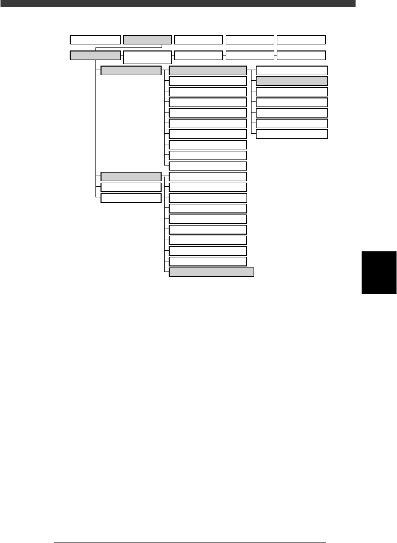
VIOS structure for Mount Info.
23547-C0-00
A1 MAIN WINDOW
A2 SUB WINDOW
A3 VIEW DATABASE NO.
A4
VISION ALIGNMENT DIC.
A5
A6
A7 FIND NEXT
A8
A9
A0 RETURN TO EDIT
B1 ADJUST ASSISTANT
B2 DATABASE UTILITY
B3
B4
DRAW THE SHAPE (CMP)
B5
B6 SET PALLET
B7 CONVEYOR UNITS
B8
B9
B0
TEACH, TRACE CONDITION
A/DISPLAY
B/UTILITY
C/EDIT_TOOL
D/FILE
PCB Info.
Mount Info.
Component Info.
Mark Info.
Blk Repeat Info.
Local Fidu.Info.
LocalBadMrkInfo.
1/OPERATION/M 2/DATA/M 3/MAINTE/M 4/SHELL/M 0/EXIT
1/EDIT_DATA
2/DATA_
GENERATOR
3/DATABASE 4/MANUAL 0/EXIT
5
-102
EPD8013110
Operation
Chapter 5
5
Creating the PCB data
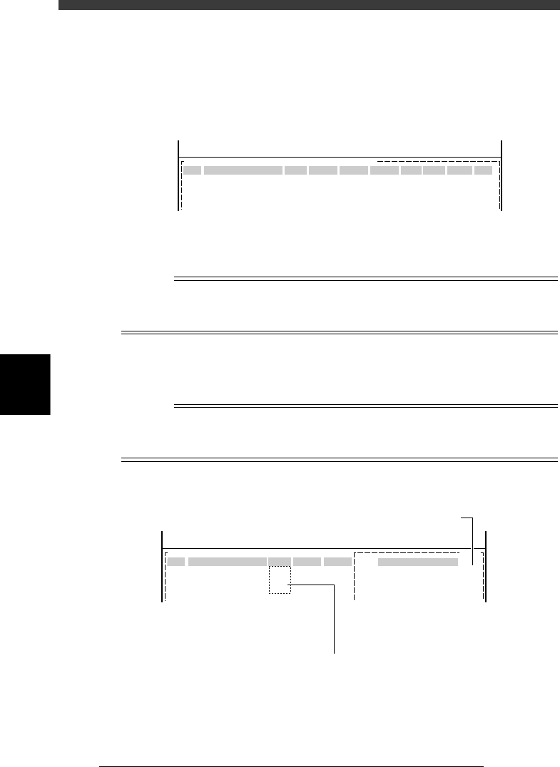
1 Open the Mount Info. screen.
Select “Mount Info.” from the edit item menu box which appears after
registering or selecting a PCB name. If an edit screen is open, press the
[F3] key (or select <2/1/A1 MAIN WINDOW>) to display the edit item
menu box.
Mount Info. screen
27538-C0-00
PCB :
SignOfLandPattern Comp
X
YR
Head
FidMk
BadMk Skip?
OBJ :Mount Info
No.
1
2
3
<<<APPLICATION>>> 2/DATA/M
<<MODE>>1/EDIT_DATA
2 Enter the land pattern name.
Enter the land pattern name or symbol (ex., R23, U12, etc.) printed on the
PCB in the SignOfLandPattern column.
Reference
If you have no material showing the land pattern names in this step, you can enter them
when you confirm and correct the mounting position as described later in “8.2 Checking
the mount information”.
3 Enter the component number.
Enter the number of the component (data No. in the component informa-
tion) to be mounted in the Comp column.
Reference
Pressing the [F4] key displays part of the Component Info. (component No., component
name, feeder set No.) in the sub-window on the right of the screen as shown below. To
close the Component Info. display, press the [F4] key again
Mount Info. and Component Info. screen
27539-C0-00
Main window: mount information Sub-window: component informatio
n
No.
1
2
3
COMPONENT NAME
R1608
R2125
R3126
OBJ:
F 20
F 21
F 22
PCB :
SignOfLandPattern
R3126
Comp
3
X
Y
OBJ :Mount Info
No.
1
2
3
<<<APPLICATION>>> 2/DATA/M
<<MODE>>1/EDIT_DATA
Feeder Set No.
Enter component No. while referring to the sub-window.
5
-103
EPD8013110
Operation
Chapter 5
5
Creating the PCB data
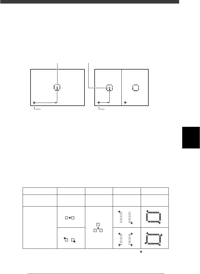
4 Enter the XY data.
For single PCBs, enter the XY coordinate data of the center of the mount-
ing position relative to the PCB origin (see “6.2” in this chapter). In the
case of multi-block PCBs, enter the position data relative to the block
repeat No.1 (see Chapter 6).
You can also use the teaching function to enter the XY coordinate data as
explained below.
Mounting position relative to the PCB origin
23548-C0-00
Block 1 Block 2
Center of mounting position
PCB origin Block repeat No.1
To perform teaching to enter the XY coordinate data, proceed as follows:
1. Move the cursor to the “X” or “Y” column on the Mount Info. screen.
2. Manipulate the joystick to move the teaching camera so that the cross
cursor on the vision monitor is aligned with the teaching position.
For single point input, press the [F10] key twice.
For multi-point inputs, press the [SHIFT]+[F10] keys twice at the first
point and once at the second and third points, then press the [F10] key
only at the final point.
Typical teaching methods are shown in the table below. Use any desired
teaching method.
Teaching method for each component
25516-C0-00
Component type
Teaching method
Teaching point
CHIP Tr. SOP
QFP
: Teaching point
1 or 2-point
input
1-point
input
2 or 4-point
input
2 or 4-point
input