YV180X_Ope_E.pdf - 第201页
5 -125 EPD8013110 Operation Chapter 5 5 Creating the PCB data 10.3.1 PCB data err or T ake the following measure if an error occurs while loading the PCB data. 1 Check the error message. If an error occurs, check the err…

5
-124
EPD8013110
Operation
Chapter 5
5
Creating the PCB data
10.3 Error countermeasures during
mounting test
If any error occurs during machine operation, take necessary corrective
action as explained below.
1 Press the [ESC] key to stop the alert sound.
2 Check the error message.
The error message is displayed on the operation monitor, so check and
make a note of the contents and error code.
3 Press the [ESC] key again to clear the error message.
4 Take corrective action.
To take corrective action, refer to the following sections “10.3.1” to
“10.3.5” which describe typical errors and the countermeasures.
5
-125
EPD8013110
Operation
Chapter 5
5
Creating the PCB data
10.3.1 PCB data error
Take the following measure if an error occurs while loading the PCB data.
1 Check the error message.
If an error occurs, check the error message displayed on the operation
monitor.
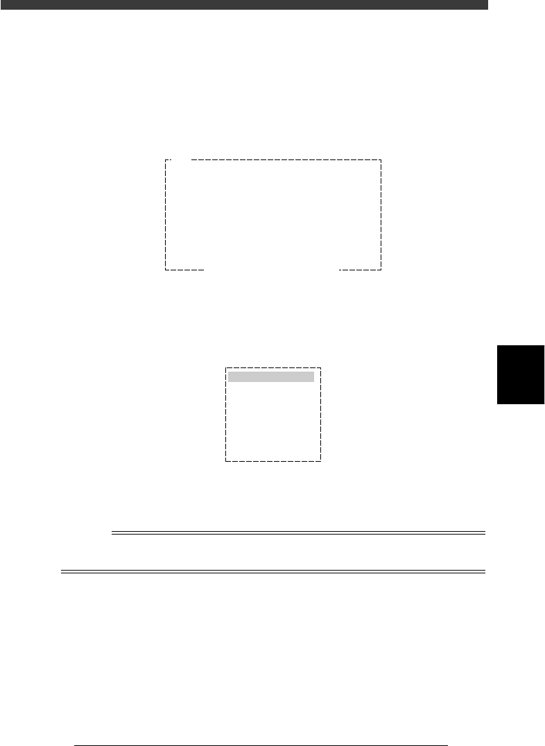
PCB DATA ERROR screen example
27555-C0-00
E150
PCB DATA ERROR
Illegal component shape data
or component data is not defined.
Component data ……………………
If this component is :FixCmpRef.
execute "FIX COMP. MATCH" in "DATA_GENERATOR"
Input the "Alignment Type" in "Component Info."
If executing "AUTO DISTRIBUTION" , execute the
optimization for each machine.
Ensure SAFETY and hit [ ENTER ] key.
2 Select the data and make corrections.
Select <1/2/PRD.DATA> and press the [ENTER] key, then select the data to
be corrected. Make necessary corrections according to the error message.
Edit item selection box
27556-C0-00
OBJECT
PCB Info.
Mount Info.
Component Info.
Mark Info.
Blk Repeat Info.
Local Fidu. Info.
Local BadMrk Info.
3 Confirm the corrected data.
Run the <1/2/C8 PCB DATA CHECK> command, and confirm that the
error has been corrected.
n
NOTE
The data check carried out with <1/2/C8 PCB DATA CHECK> is the same as that carried
out when executing the <1/1/D3 SWITCH PCB> command.
5
-126
EPD8013110
Operation
Chapter 5
5
Creating the PCB data
10.3.2 Fiducial mark recognition error
If an error occurs during fiducial mark recognition or no mark can be
recognized, correct the data with the procedure below.
1 Enter the teaching mode.
If a fiducial mark recognition error occurs during automatic operation, the
following error message appears. Then, press the [F10] key to enter the
teaching mode.
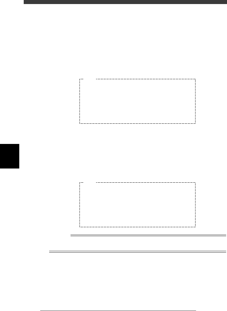
Mark recognition error message screen
27557-C0-00
E56
MARK DETECTION ERROR
Failed to detect frfined mark.
(MarkNo. 1)
Do you execute VISION-CURSOR-TEACHING
[F10] key to execute
Any othr key to abort.
2 Perform vision cursor teaching.
When the teaching mode is entered, the following message is displayed.
Perform vision cursor teaching for the target mark while referring to the
procedure explained in “12. Teaching and trace” in this chapter.
Press the [ENTER] key after teaching, the teaching position coordinates are
then entered and the machine resumes automatic operation.
Vision cursor teaching screen
27558-C0-00
E57
VISION-CURSOR-TEACHING
Please teach fiducial mark while looking
VISION-MONITOR
[ESC] : Abort
[ENTER] : Teaching
[Arrows] : Moving at TEACH-WINDOW
[SHIFT]+[Arrows] : Moving at TEACH-WINDOW
[TAB] : Changing at TEACH-WINDOW
Reference
The initial size of the teaching window displayed when the teaching mode is entered is the
size specified by the “MarkOutSize” parameter in the mark information.