YV180X_Ope_E.pdf - 第282页
6 -47 EPD8013110 Operation Chapter 6 6 Using various functions 7. Self pr oduction contr ol Self production control allows the machine to identify specified PCBs by recognizing the mark on the PCB, from among dif ferent …
6
-46
EPD8013110
Operation
Chapter 6
6
Using various functions
6
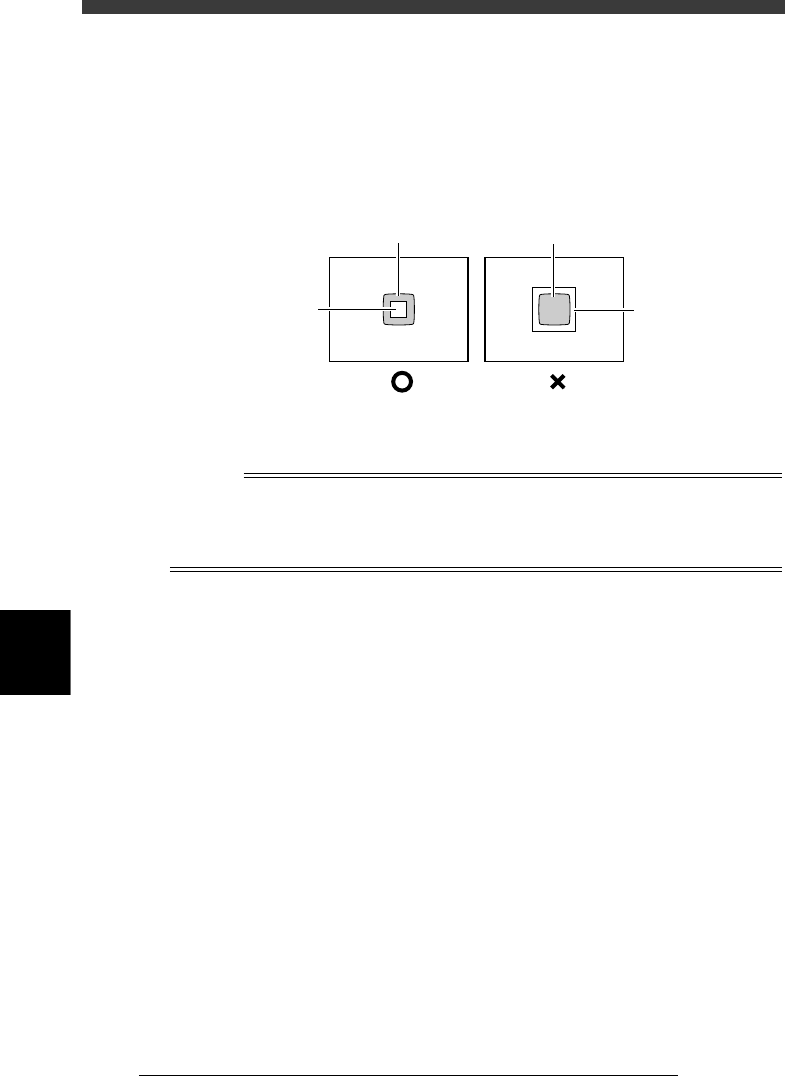
6. On the vision monitor, you will see a square window with the length of
one side specified by the “Search Area” parameter in the Vision Info.
sub-window. Since the average brightness in this square window is
measured to determine the badmark threshold level, the square
window must be positioned within the badmark. If the square window
is larger than the badmark, reduce the “Search Area” parameter value
in the Adjust Assist Items.
Badmark detection area (Search Area)
23617-C0-00
Badmark
Mark search
area
Badmark
Mark search
area
4 Execute the EXIT command.
Exit the Adjust Assistant and return to the Mark Info. screen.
n
NOTE
When you quit the Adjust Assistant, the optimized result (“Mark Threshold” value) will
automatically be entered for the “Mark Threshold” parameter on the Vision Info. sub-
window in the mark information. For more details on threshold levels, see “4.3 Executing
the Adjust Assistant commands” in Chapter 5.
6
-47
EPD8013110
Operation
Chapter 6
6
Using various functions
7. Self production control
Self production control allows the machine to identify specified PCBs by
recognizing the mark on the PCB, from among different types of PCBs
which are consecutively supplied on the conveyor.
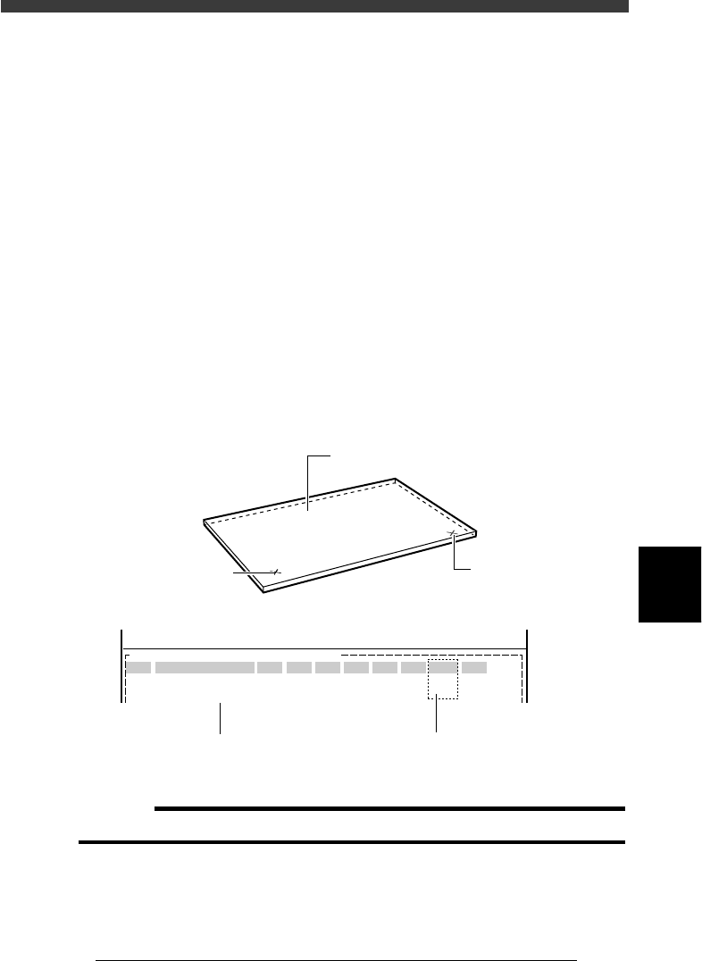
For example, when you want to mount different components between the
front and back sides of a PCB, affix badmark A to the front side and
badmark B to the back side, and register their information in the Mark Info.
and also Local Badmark Info. Then, register the mount data on both sides
of the PCB in the Mount Info. and specify badmark A in the “BadMk”
column of components to be mounted on the front surface, while specify-
ing badmark B in the “BadMk” column of the components to be mounted
on the back side. With these settings, even when PCBs are supplied with
either the front or back side facing up, the machine identifies the front and
back sides, and mounts components only on the front side when badmark A
is recognized. Likewise, the machine mounts components only on the back
side when badmark B is recognized.
Badmarks for self production control
23618-C0-00
PCB :
SignOfLandPattern
R1005
R2125
Comp
10
12
BadMk
1
2
Skip?
Exec
Exec
OBJ :Mount Info.
No.
1
2
<<<APPLICATION>>> 2/DATA/M
<<MODE>> 1/EDIT_DATA
X
30.00
20.50
Y
45.00
10.00
R
0.00
0.00
Head
1
2
FidMk
0
0
Front or back side of PCB can be
identified by badmark No. setting
Front side badmark (A)
Back side badmark (B
)
Register the mount data for
both front and back sides
PCB
c
CAUTION
Self production control can only be used for PCBs with the same size.
6
-48
EPD8013110
Operation
Chapter 6
6
Using various functions
6
1 Register the PCB data for self production.
In order to utilize self production control you must create a combination
of PCB data (hereafter called “SELF_PROD_EXAMPLE”) which is made up
of two or more units of PCB data (for example “PCB1” and “PCB2”) which
are to be successively supplied on the conveyor.
1. Use the <2/1/D2 CREATE PCB> command to register the PCB name
“SELF_PROD_EXAMPLE” for self production.
2. After registering the PCB name, press the [F2] key to select it
(“SELF_PROD_EXAMPLE”) for data creation.
Reference
If the “PCB1” or “PCB2” data is already registered, it will prove helpful to copy either
one with the <2/1/D4 COPY PCB DATA> command and then rename it to
“SELF_PROD_EXAMPLE”.
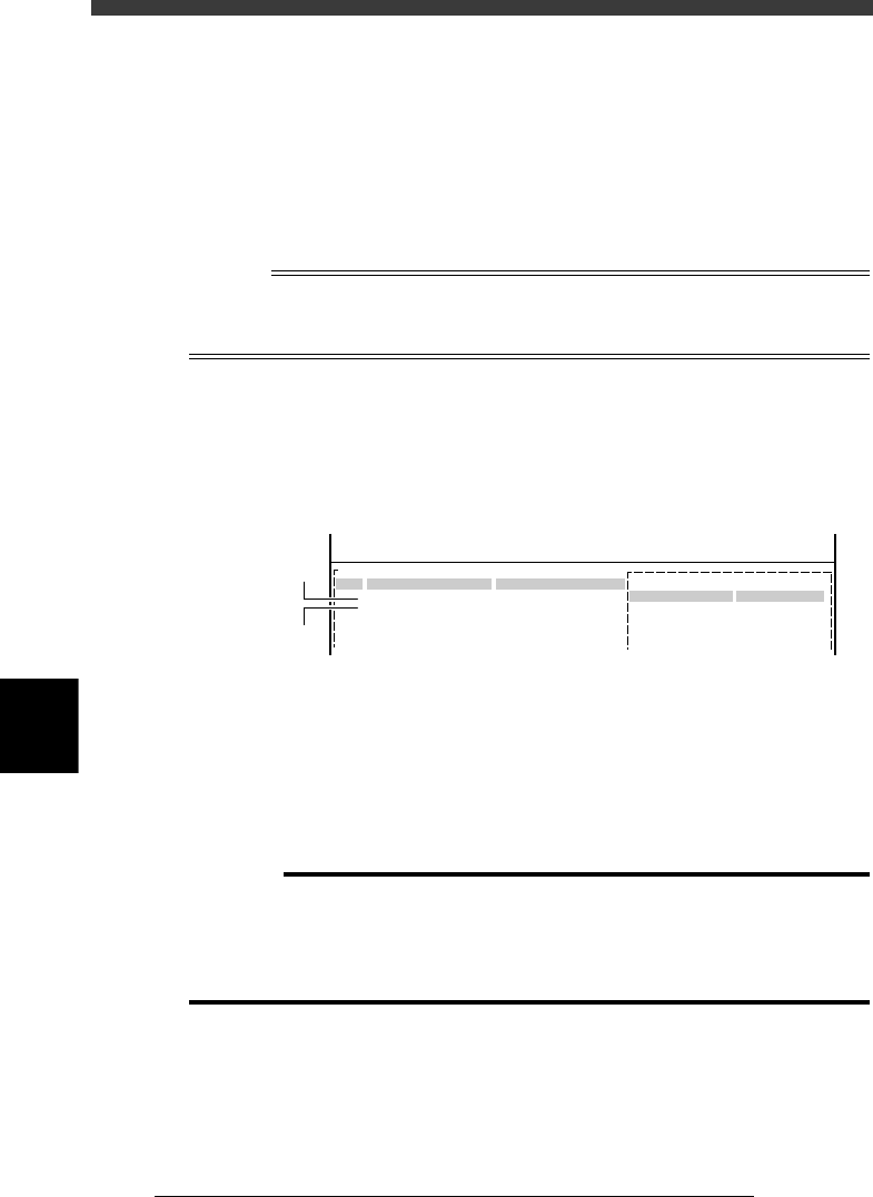
2 Create the mark information.
Open the Mark Info. screen and register the self production marks, just as
when registering normal fiducial marks. However, set the Mark Type
parameter to “Fid for Bad” and the Bad Mark Rev. parameter to “Reverse”.
Mark information settings for self production
27630-C0-00
Fid for Bad
Reverse
0
PCB:SELF_PROD_EXAMPLE
Mark Type Info.
Edit Term
Mark Type
Bad Mark Rev
DataBase Number
OBJ : Mark Info.
MARK NAME
Mark_1
Mark_2
No.
1
2
3
4
COMMENT
For PCB1
For PCB2
:
:
:
:
V
<<<APPLICATION>>> 2/DATA/M
<<MODE>> 1/EDIT_DATA
Data for PCB1
Data for PCB2
3 Create the component information
Open the Component Info. screen and register the data on all components
to be used for “PCB1” and “PCB2”. To create the component data, refer to
“3. Creating the component information” in Chapter 5.
If the component data is already registered in the “PCB1” and “PCB2”,
copying each of the data and pasting it in the “SELF_PROD_EXAMPLE” is
recommended. (Refer to “13. Data editing for production PCB” in Chapter
5 to make a copy.)
c
CAUTION
The component numbers of the copy source and copy destination must be the same in
order to paste the copied data.
If the component number is duplicated in the copy destination, change the component
number of either of the PCB data, and then change the “Component” in the Mount
Info. to match this change.