YV180X_Ope_E.pdf - 第78页
6. Creating the PCB information ............................................ 5-89 6.1 Creating procedure ................................................................. 5-91 6.2 PCB origin .............................…

Chapter 5
Creating the PCB data
continued...
1. Overview ............................................................................. 5-3
2. Registering and selecting the PCB name............................... 5-5
2.1 Registering PCB names ............................................................. 5-6
2.2 Selecting the PCB name ........................................................... 5-8
3. Creating the component information ................................. 5-10
3.1 Creating procedure................................................................. 5-12
3.2 Various parameter settings ...................................................... 5-15
3.3 Chip components ................................................................... 5-16
3.3.1 Standard chip components
(box type chip resistors and capacitors) 5-16
3.3.2 Melf components (cylindrical components) 5-23
3.4 IC components ....................................................................... 5-27
3.4.1 Mini-mold transistor/SOT 5-27
3.4.2 SOP components 5-32
3.4.3 QFP components 5-37
3.5 Ball lead components ............................................................. 5-42
3.5.1 Simple BGA 5-42
3.5.2 BGA components (BGA setting) 5-46
3.6 Connector components .......................................................... 5-54
3.6.1 Connectors 5-54
3.7 Adjust Assistant commands .................................................... 5-58
3.8 Setting the stick feeder component data ................................. 5-65
3.8.1 When optimizing the feeder set positions 5-65
3.8.2 When not optimizing the feeder set positions 5-69
3.9 Registration location of component data ................................ 5-71
4. Creating the mark information ........................................... 5-72
4.1 Creating procedure................................................................. 5-74
4.2 Various parameter settings ...................................................... 5-76
4.3 Adjust Assistant commands .................................................... 5-82
5. Clamping the PCB .............................................................. 5-86
This chapter explains the basic procedures for creating or editing
PCB data and also making test-mount of components in order to
check the PCB data.
6. Creating the PCB information ............................................ 5-89
6.1 Creating procedure................................................................. 5-91
6.2 PCB origin .............................................................................. 5-96
6.2.1 Normal PCB origin position setting 5-97
6.2.2 Setting the PCB origin at a position other than the locate pin 5-98
6.2.3 Setting the PCB origin for multi-block PCB 5-99
7. Creating the mount information....................................... 5-100
8. Checking the data ............................................................ 5-106
8.1 Checking the component information .................................. 5-106
8.2 Checking the mount information .......................................... 5-107
9. Data optimization ............................................................ 5-111
9.1 Selecting the data ................................................................. 5-112
9.2 Setting optimization conditions ............................................ 5-113
9.3 Optimizing the data ............................................................. 5-116
10. Mounting test and data correction ................................... 5-117
10.1 Making setups for mounting test ........................................... 5-118
10.2 Starting the test mount .......................................................... 5-121
10.3 Error countermeasures during mounting test ......................... 5-124
10.3.1 PCB data error 5-125
10.3.2 Fiducial mark recognition error 5-126
10.3.3 Component pickup error 5-128
10.3.4 Component recognition error 5-130
10.3.5 Component mount error 5-131
10.4 Correcting the data after mounting test ................................. 5-133
11. Data backup ..................................................................... 5-136
11.1 Creating a PCB data disk ...................................................... 5-137
11.2 Data backup......................................................................... 5-139
12. Teaching and trace ........................................................... 5-140
12.1 Trace .................................................................................... 5-140
12.2 Teaching ............................................................................... 5-142
12.2.1 Point teaching 5-142
12.2.2 Vision cursor teaching 5-143
12.3 Automatic trace .................................................................... 5-147
13. Data editing for production PCB ...................................... 5-148
13.1 Data editing ......................................................................... 5-148
13.1.1 Copying the specified range 5-148
13.1.2 Deleting the specified range 5-150
13.1.3 Inserting one line 5-151
13.1.4 Deleting one line 5-152
13.2 Data replace ......................................................................... 5-153
13.2.1 Data replace in mount information 5-153
13.2.2 Data replace in component information 5-156
13.3 Data sort .............................................................................. 5-159
5
-3
EPD8013110
Operation
Chapter 5
5
Creating the PCB data
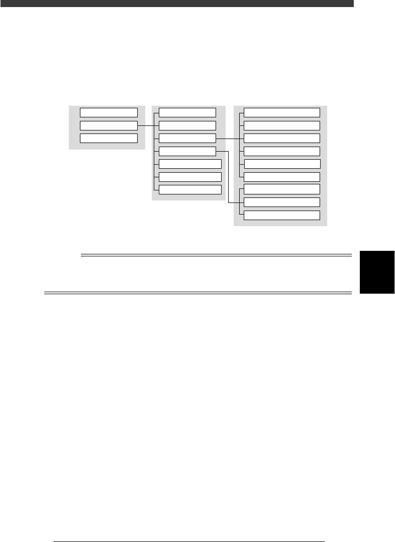
1. Overview
The PCB data is indexed by means of each individual PCB name. Each
PCB type consists of various information as shown below.
Data management for each PCB
23501-C0-00
PCB NAME MAIN WINDOW SUB WINDOW
PCB1
PCB2
PCB3
PCB Info.
Mount Info.
Component Info.
Mark Info.
Block Repeat Info.
Local Fidu. Info.
Local BadMrk Info.
1. BASIC INFO.
2. OPTION INFO.
3. PICK & MOUNT INFO.
4. DUMP INFO.
5. VISION INFO.
6. SHAPE INFO.
Mark Type Info.
Mark size Info.
Vision Info.
n
NOTE
This section describes basic methods for creating PCB data so that you will understand
what data is needed for what item. After you have obtained a complete understanding of
these methods, begin actual work according to the desired method.