YV180X_Ope_E.pdf - 第166页
5 -90 EPD8013110 Operation Chapter 5 5 Creating the PCB data VIOS structure for “PCB Info.” 23539-C0-00 A1 MAIN WINDOW A2 SUB WINDOW A3 VIEW DATABASE NO. A4 VISION ALIGNMENT DIC. A5 A6 A7 FIND NEXT A8 A9 A0 RETURN TO EDI…
5
-89
EPD8013110
Operation
Chapter 5
5
Creating the PCB data
6. Creating the PCB information
This section describes how to create PCB information such as for PCB size
and production methods.
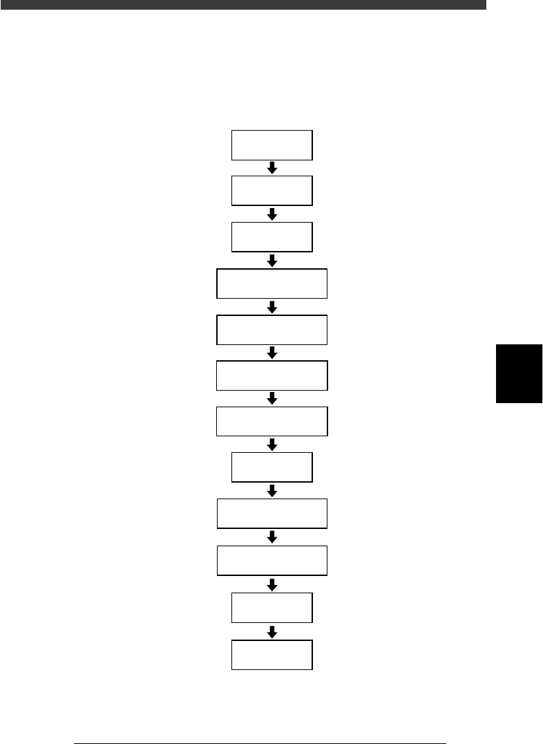
Flow chart for creating PCB information
23538-C0-00
Input
PCB Origin
Open
PCB Information
Input PCB Size
Set PCB Fiducial
Set BLOCK Fiducial
Set PCB Badmark
Set BLOCK Bad mark
Input
PCB Comment
Set
Pcb/Schedule/Block
Set
Unloader Count/Max
Set operation
conditions
Save data
5
-90
EPD8013110
Operation
Chapter 5
5
Creating the PCB data
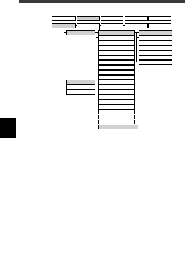
VIOS structure for “PCB Info.”
23539-C0-00
A1 MAIN WINDOW
A2 SUB WINDOW
A3 VIEW DATABASE NO.
A4
VISION ALIGNMENT DIC.
A5
A6
A7 FIND NEXT
A8
A9
A0 RETURN TO EDIT
B1 ADJUST ASSISTANT
B2 DATABASE UTILITY
B3
B4
DRAW THE SHAPE (CMP)
B5
B6 SET PALLET
B7 CONVEYOR UNITS
B8
B9
B0
TEACH, TRACE CONDITION
A/DISPLAY
B/UTILITY
C/EDIT_TOOL
D/FILE
PCB Info.
Mount Info.
Component Info.
Mark Info.
Blk Repeat Info.
Local Fidu.Info.
LocalBadMrkInfo.
1/OPERATION/M 2/DATA/M 3/MAINTE/M 4/SHELL/M 0/EXIT
1/EDIT_DATA
2/DATA_
GENERATOR
3/DATABASE 4/MANUAL 0/EXIT
5
-91
EPD8013110
Operation
Chapter 5
5
Creating the PCB data
6.1 Creating procedure
1 Open the PCB Info. screen.
Select “PCB Info.” from the edit item menu box which appears after
registering or selecting a PCB name. If an edit screen is open, press the
[F3] key (or select <2/1/A1 MAIN WINDOW>) to display the edit item
menu box.
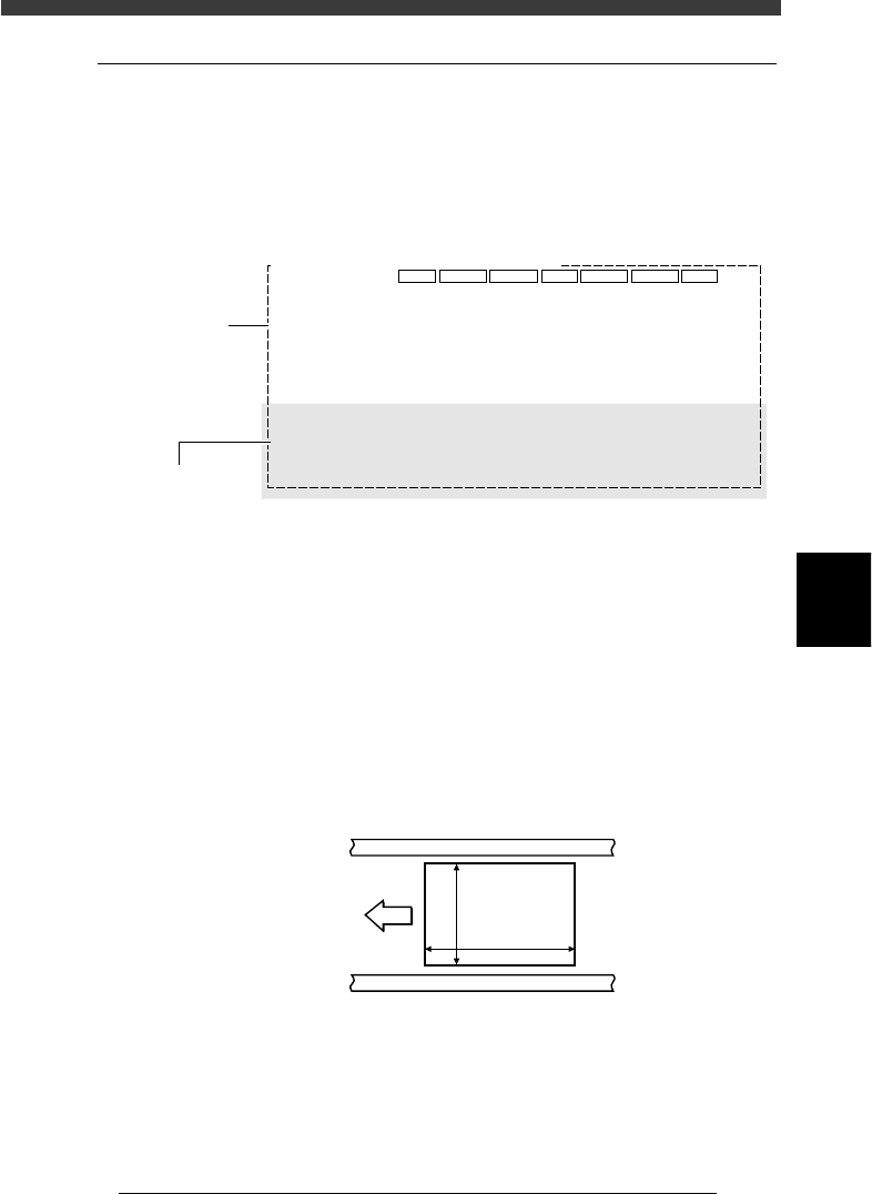
PCB Info. screen
27537-D8-00
PCB: OBJ :PCB Info.
MARK
1
1
1
6
X/X1
0.00
240.00
0.00
5.00
0.00
15.00
0
0
Y/Y1
0.00
175.00
10.00
5.00
0.00
5.00
0
0
MRK2
0
0
X2
1.6
230.00
215.00
Y2
160.00
77.50
Skip?
-1
NotUse
NotUse
NotUse
NotUse
Exec
NoCheck
IgnoreErr
PcbFixDevice
Pre-FixTimer
Trans-Height
Conv. Timer
Precede Pick
Pin+PushUP
0.00
0
0.00
Not Use
Local Fiduc.
LocalBadmark
Retry Seq.
TrayPrecede.
Sp.Function
Not Use
Not Use
Group
USe
Not Use
Mount
Vacuum Check
Aligment
PCB Origin
PCB Size
PCB Fiducial
BLOCK Fiducial
PCB Badmark
BLOCK Badmark
PCB Comment
Pcb/Schedule/Block
Unloader Count/Max
Operation condition
setting area
PCB parameters
2 Enter “PCB Origin”.
The PCB origin is the reference XY position on the PCB. Refer to “6.3 PCB
origin” in this chapter for more details.
3 Enter “PCB Size”.
Enter the length of the PCB in the XY directions in millimeters. The
conveyor width (W-axis) will be adjusted according to the Y length in
automatic operation.
X coordinate: Length in the PCB flow direction
Y coordinate: Length in the conveyor width direction when the PCB is
set on the conveyor
PCB Size
23540-C0-00
X [mm]
Y [mm]
PCB
Direction of
PCB flow
4 Enter the thickness of the PCB.
Enter the thickness of the PCB in the “X2” column of the PCB Size.