YV180X_Ope_E.pdf - 第277页
6 -42 EPD8013110 Operation Chapter 6 6 Using various functions 6 4 Open the PCB Info. screen and set the local badmark function. Press the [F3] key to display the edit item menu box again, then select “ PCB Info. ” and s…
6
-41
EPD8013110
Operation
Chapter 6
6
Using various functions
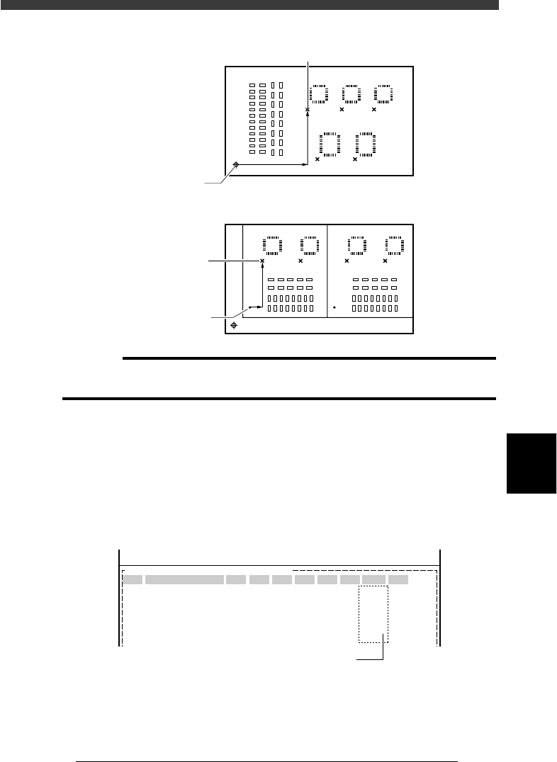
Local badmark XY coordinates
23615-C0-00
X
X
Y
Y
<Relative to PCB origin>
<Relative to block repeat No.1>
Badmark
Badmark
PCB origin
Block repeat
c
CAUTION
You can enter the XY coordinates of local badmarks by teaching. In this case, set the
PCB origin (block repeat) data correctly before teaching.
3 Open the Mount Info. screen and specify the badmark.
1. Press the [F3] key to display the edit item menu box, then select
“Mount Info.”.
2. Move the cursor to the data line for which you want to set the badmark
function, then enter the mark data No. you have registered in the Local
BadMrk Info., in the “BadMk” column of the selected data line.
Local badmark settings
27623-C0-00
PCB :
SignOfLandPattern Comp X Y R Head FidMk BadMk
1
2
3
4
5
Skip?
OBJ :Mount Info.
No.
1
2
3
4
5
<<<APPLICATION>>> 2/DATA/M
<<MODE>> 1/EDIT_DATA
Enter one piece of local badmark data
for one piece of mount data.

6
-42
EPD8013110
Operation
Chapter 6
6
Using various functions
6
4 Open the PCB Info. screen and set the local badmark
function.
Press the [F3] key to display the edit item menu box again, then select
“PCB Info.” and set the “LocalBadmark” parameter to “Use”.
Setting the local badmark function on the PCB Info. screen
27624-C0-00
PCB :
LocalBadmark Use
OBJ : PCB Info.
<<<APPLICATION>>> 2/DATA/M
<<MODE>> 1/EDIT_DATA
Set to “Use”.
5 Save the data.
Press the [ESC] key to exit the current edit screen, then select <2/1/D8
SAVE PCB DATA> and press the [ENTER] key.
n
NOTE
The local badmark function can also be utilized for automatic switching of PCB types. See
“7. Self production control” for more details.
6
-43
EPD8013110
Operation
Chapter 6
6
Using various functions
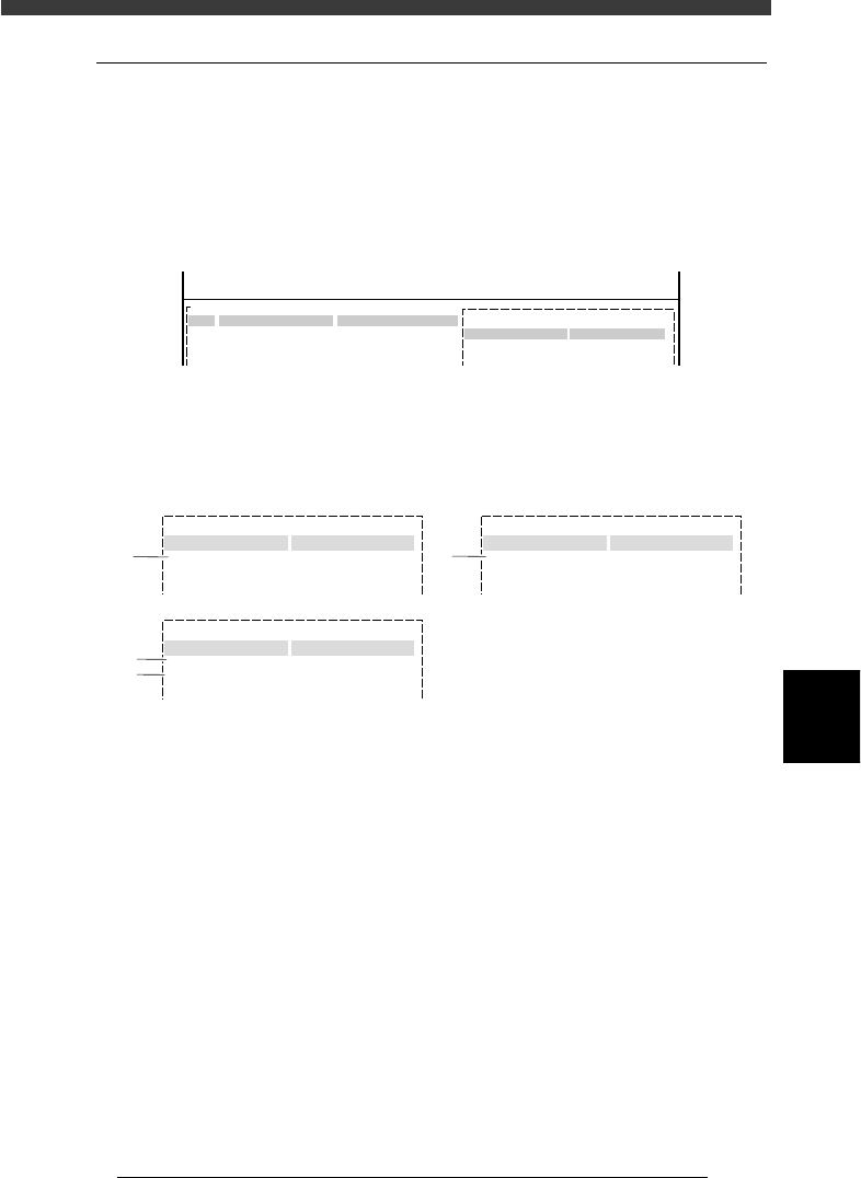
6.3 Creating the badmark information
To create the badmark information, follow the steps below.
1 Create the mark information.
In <2/1/EDIT_DATA> mode, open the Mark Info. screen for which you
want to use the badmark function. Enter the mark name and comment
along a blank line.
Badmark registration screen (Mark Info. screen)
27625-C0-00
PCB:
Mark Type Info.
Edit Term
OBJ : Mark Info.
MARK NAME
BADMARK
No.
1
2
3
COMMENT
For PCB
:
V
<<<APPLICATION>>> 2/DATA/M
<<MODE>> 1/EDIT_DATA
2 Set the parameters in sub-windows.
While switching the sub-windows by pressing the [F4] key, set the
following parameters.
Badmark parameter settings
27626-C0-00
:
:
Mark Type Info.
Edit Term
Mark Type
DataBase Number
:
:
:
153
Mark size Info.
Edit Term
Search Area 4.00
Vision Info.
Edit Term
Surface Type
Mark Threshold
:
:
:
Reflect
220
Badmark
1
3
4
2
Mark Type Info. parameter
1. Mark Type
Set to “Badmark”.
Mark Size Info. parameter
2. Search Area
This parameter specifies the size of an square area in which a mark is
searched. The setting value can be 0.00 to 9.99 (in millimeters) which
represents the length of one side. The larger this value, the larger the
search area.
The search area must be smaller than the badmark to be detected,
because the machine detects the badmark depending on whether it is
reflective or non-reflective within the specified search area.