Q170226E01.pdf - 第314页
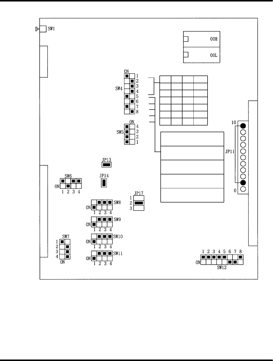
8.3 List of Jumper Switch Settings SERVICE MANUAL RH5 8.3−17 DA3SEC−85−540−B0 Switch List Switch No. Function Description 1 Reset signal generation 5 2 NMI signal generation 5 3 4 Switch for setting (x 8) 2 5 Switch for …
RH5
8.3 List of Jumper Switch Settings
SERVICE MANUAL
8.3−16
DA3SEC−85−540−B0
8.3.4 MIOE (I) Board Setting
SW1: Generates reset signal.
1 2 3 BPS
0 0 0 9600
1 0 0 4800
0 1 0 2400
1 1 0 1200
0 0 1 600
1 0 1 300
4: Brake character
ON: Output
OFF: Not output
5: Checksum
ON: Yes
OFF: No
6: R recommend
ON: Output
OFF: No output
7: Time out
ON: Yes
OFF: No
8: End code
ON: CR
OFF: ETX
1:
2:
3:
4:
5:
6:
7:
8:
=REFERENCE=
JP17 (FDD) setting
For PC98 series For IBM PC series
JP17 − 1: Open JP17 − 1: Open
JP17 − 2: Short JP17 − 2: Open
JP17 − 3: Open JP17 − 3: Open

8.3 List of Jumper Switch Settings
SERVICE MANUAL
RH5
8.3−17
DA3SEC−85−540−B0
Switch List
Switch No. Function Description
1 Reset signal generation 5
2 NMI signal generation 5
3
4 Switch for setting (x 8) 2
5 Switch for setting(x 4) 2
6 Leader start signal switching 4
7 TTY output data switching 4
8 TTY input data switching 4
9 TTY input data switching 4
10 Busy signal switching 4
11 Busy signal switching 4
12 Dual port RAM address setting on the bus side 1
Jumper List
Jumper
No.
Function Description
1 Selects RXC of HOST 4
2 Selects TXC of HOST 4
3 Selects CCLK output 6
4 Selects BCLK output 6
5 Selects TXC/RXC for TTY 4
6 Selects CTS for TTY 4
7
8 Selects RTS for TTY 4
9 Select 82289 6
10 Selects BPRO output 6
11 Selects P2 bus interrupt level 7
12 Selects WD37C65 3
13 Terminates READER START signal 4
14 Pull−up to +12V volts for TTY input data 4
15 Selects TXD for TTY 4
16 Selects RXD for TTY 4
17 Jumper (x 3) for setting 3
18 Selects clock SIO1/2 4
19 Selects TXC/RXC for SIO1 4
20 Selects TXC/RXC for SIO2 4
RH5
8.3 List of Jumper Switch Settings
SERVICE MANUAL
8.3−18
DA3SEC−85−540−B0
Dual port RAM
There is a dual port 64 KB (SRAM) on the board. It is used to communicate between the local bus and
an external bus (P2 bus).
The address mapping seen from the local bus is from B000H to BFFFFH. The mapping seen from the
external bus is a 64 KB segment set with SW12 on the board.
SW12
1234 5678
ON
ADR23 − ADR20 AD13 − AD10 ADRF − ADR0
ON = “1”
OFF = “0”
In the above example, the address mapping seen from the external bus is the absolute address from
060000H to 06FFFH, 64 KB.