Q170226E01.pdf - 第315页
RH5 8.3 List of Jumper Switch Settings SERVICE MANUAL 8.3−18 DA3SEC−85−540−B0 Dual port RAM There is a dual port 64 KB (SRAM) on the board. It is used to communicate between the local bus and an external bus (P2 bus). Th…
8.3 List of Jumper Switch Settings
SERVICE MANUAL
RH5
8.3−17
DA3SEC−85−540−B0
Switch List
Switch No. Function Description
1 Reset signal generation 5
2 NMI signal generation 5
3
4 Switch for setting (x 8) 2
5 Switch for setting(x 4) 2
6 Leader start signal switching 4
7 TTY output data switching 4
8 TTY input data switching 4
9 TTY input data switching 4
10 Busy signal switching 4
11 Busy signal switching 4
12 Dual port RAM address setting on the bus side 1
Jumper List
Jumper
No.
Function Description
1 Selects RXC of HOST 4
2 Selects TXC of HOST 4
3 Selects CCLK output 6
4 Selects BCLK output 6
5 Selects TXC/RXC for TTY 4
6 Selects CTS for TTY 4
7
8 Selects RTS for TTY 4
9 Select 82289 6
10 Selects BPRO output 6
11 Selects P2 bus interrupt level 7
12 Selects WD37C65 3
13 Terminates READER START signal 4
14 Pull−up to +12V volts for TTY input data 4
15 Selects TXD for TTY 4
16 Selects RXD for TTY 4
17 Jumper (x 3) for setting 3
18 Selects clock SIO1/2 4
19 Selects TXC/RXC for SIO1 4
20 Selects TXC/RXC for SIO2 4
RH5
8.3 List of Jumper Switch Settings
SERVICE MANUAL
8.3−18
DA3SEC−85−540−B0
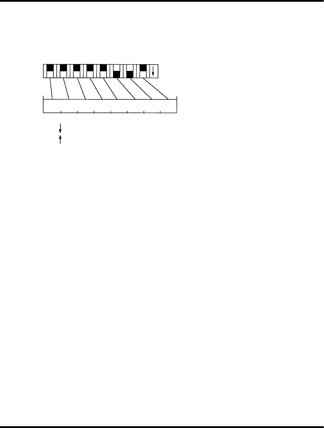
Dual port RAM
There is a dual port 64 KB (SRAM) on the board. It is used to communicate between the local bus and
an external bus (P2 bus).
The address mapping seen from the local bus is from B000H to BFFFFH. The mapping seen from the
external bus is a 64 KB segment set with SW12 on the board.
SW12
1234 5678
ON
ADR23 − ADR20 AD13 − AD10 ADRF − ADR0
ON = “1”
OFF = “0”
In the above example, the address mapping seen from the external bus is the absolute address from
060000H to 06FFFH, 64 KB.

8.3 List of Jumper Switch Settings
SERVICE MANUAL
RH5
8.3−19
DA3SEC−85−540−B0
System port MB89363B
This port is provided to perform I/O for data that each LSI can’t process by itself.
I/O port
address
Data
Bit
IN/OUT Signal Logic “0” Logic “1”
D7 IN 8onSW4 ON OFF
D6 IN 7onSW4 ON OFF
D5 IN 6onSW4 ON OFF
20H
D4 IN 5onSW4 ON OFF
20H
D3 IN 4onSW4 ON OFF
D2 IN 3onSW4 ON OFF
D1 IN 2onSW4 ON OFF
D0 IN 1onSW4 ON OFF
D7 IN Host interface CI signal Call accepted Call−not−
accepted
D6 IN Host interface CTS signal Clear to send Not clear to
send
22H
D5 IN Host interface CD signal Receive carrier
detection ON
Receive carrier
detection OFF
22H
D4 IN WD33C93 INTRQ signal Not interrupt Interrupted
D3 IN NMI factor SW YES NO
D2 IN NMI factor PFIN NO YES
D1 IN NMI factor WDT NO YES
D0 IN NMI factor ERROR NO YES
D7 OUT RAM bank switching SRAM DRAM
D6 OUT Printer strobe signal mask Release Mask
D5 OUT TTY leader start signal ON OFF
D4 OUT NMI factor mask signal Release Mask
24H
D3 OUT Buzzer output (externally connected at
CN6)
ON OFF
D2 OUT Enable interrupt from host TRY Disabled Enable
D1 OUT Enable interrupt from host EMP Disabled Enable
D0 OUT Enable interrupt from host RRY Disabled Enable
26H Mode setting 92H