Q170226E01.pdf - 第332页
8.3 List of Jumper Switch Settings SERVICE MANUAL RH5 8.3−35 DA3SEC−85−540−B0 Multibus interface (1) Dual port RAM This board cannot directly access to the multibus. (slave mode only). Communications with the main CPU ca…
RH5
8.3 List of Jumper Switch Settings
SERVICE MANUAL
8.3−34
DA3SEC−85−540−B0
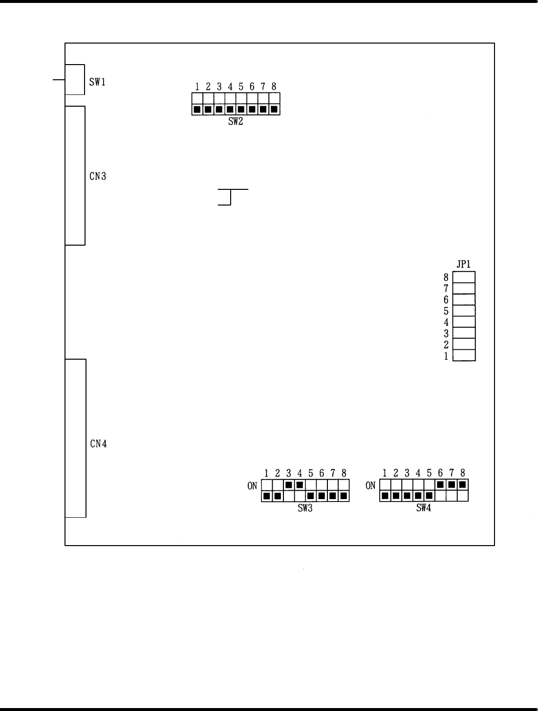
8.3.6 APC Board Setting
SW1: Reset SW
SW2: For interrupt setting
SW3: Address setting on the multibus in dual port RAM.
SW4:
8.3 List of Jumper Switch Settings
SERVICE MANUAL
RH5
8.3−35
DA3SEC−85−540−B0
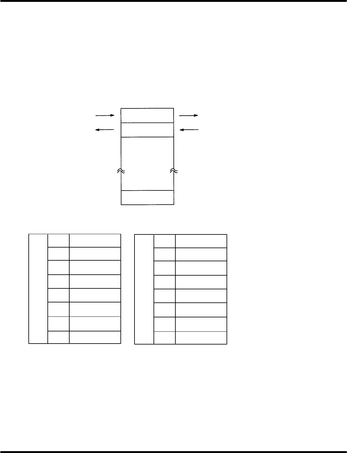
Multibus interface
(1) Dual port RAM
This board cannot directly access to the multibus. (slave mode only).
Communications with the main CPU can be done passing through the dual port RAM on this board. It
is possible to send the interrupt notification to the main CPU through the multibus interrupt line, by
writing the interrupt into the 7FE address (offset address) from the MPU (64180) on this board.
This factor will be released by reading−out the same address on the main CPU.
Similarly, the interrupt will be notified through INT0 of the MPU on this board, by writing the interrupt
into the 7FF address from CPU. This factor will be released by reading−out the same address on the
internal MPU.
Always bite−access to the host CPU.
For details, see the MB8421 manual.
Host CPU side
Internal CPU side
7FFH
7FEH
000H
The address map seen from the host CPU is set with DIP SW3 and SW4 on the board.
SW3
ON: 1
OFF: 0
ADRF
1
2
3
4
5
6
7
8
ADRE
ADRD
ADRC
ADRB
Not used
Not used
Not used
SW4
ADR23
1
2
3
4
5
6
7
8
ADR22
ADR21
ADR20
AD13
AD12
AD11
AD10
RH5
8.3 List of Jumper Switch Settings
SERVICE MANUAL
8.3−36
DA3SEC−85−540−B0
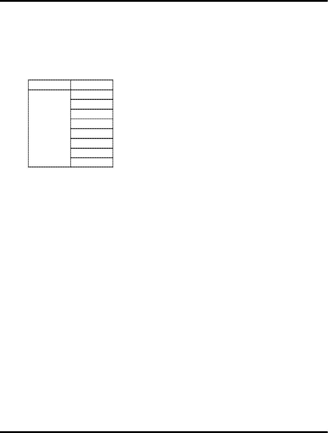
(2) Interrupt
The multibus interrupt lines are used on this board as described in the following.
INT3: The NMI interrupt on this board occurs as the error interrupt.
INT6: The interrupt occurs on this board as the end interrupt.
INT7: The interrupt is output from this board as the dual port RAM interrupt notification.
Each of the interrupt lines can be used by shorting JP1 (short pin) on this board.
Pin
Interruption
JP1−1 INT0
JP1−2 INT1
JP1−3 INT2
JP1−4 INT3
JP1−5 INT4
JP1−6 INT5
JP1−7 INT6
JP1−8 INT7