Q170226E01.pdf - 第328页
8.3 List of Jumper Switch Settings SERVICE MANUAL RH5 8.3−31 DA3SEC−85−540−B0 8.3.5 SEQ−SE (I) Board Setting DST−S board Firmware H Firmware L

RH5
8.3 List of Jumper Switch Settings
SERVICE MANUAL
8.3−30
DA3SEC−85−540−B0
Bus interrupt
From this board, it is possible to notify another board of the interrupt and input a notification from another
board as the interrupt, by going through the P2 bus interrupt notification line (line 8 of INT0−INT7).
Furthermore, a dual port interrupt can be done by writing into the specified memory area on this board.
(1) Interrupt notification line and setting
The P2 is connected to interrupt notification line with JP11.
P2 bus
JP11
INT7 A13
INT6 B13
INT5 C13
INT4 A14
INT3 B14
INT2 C14
INT1 A15
INT0 B15
ERROR
IR3 (Command interrupt)
DENT notification
7
6
5
4
3
2
1
0
8
9
10
(2) Command interrupt
A notification from another board can be notified as the interrupt by connecting 0−7 with 9 of JP11.
The interrupt is notified to level 3 of the master 8259A.
(3) Dual port interrupt
Writing the optional data into the last four bytes (FFFC
H
to FFFF
H
) in the segment (64 K) setting with
SW12 as explained in dual port RAM enables the interrupt to notify to level 5 of the master 8259A.
8.3 List of Jumper Switch Settings
SERVICE MANUAL
RH5
8.3−31
DA3SEC−85−540−B0
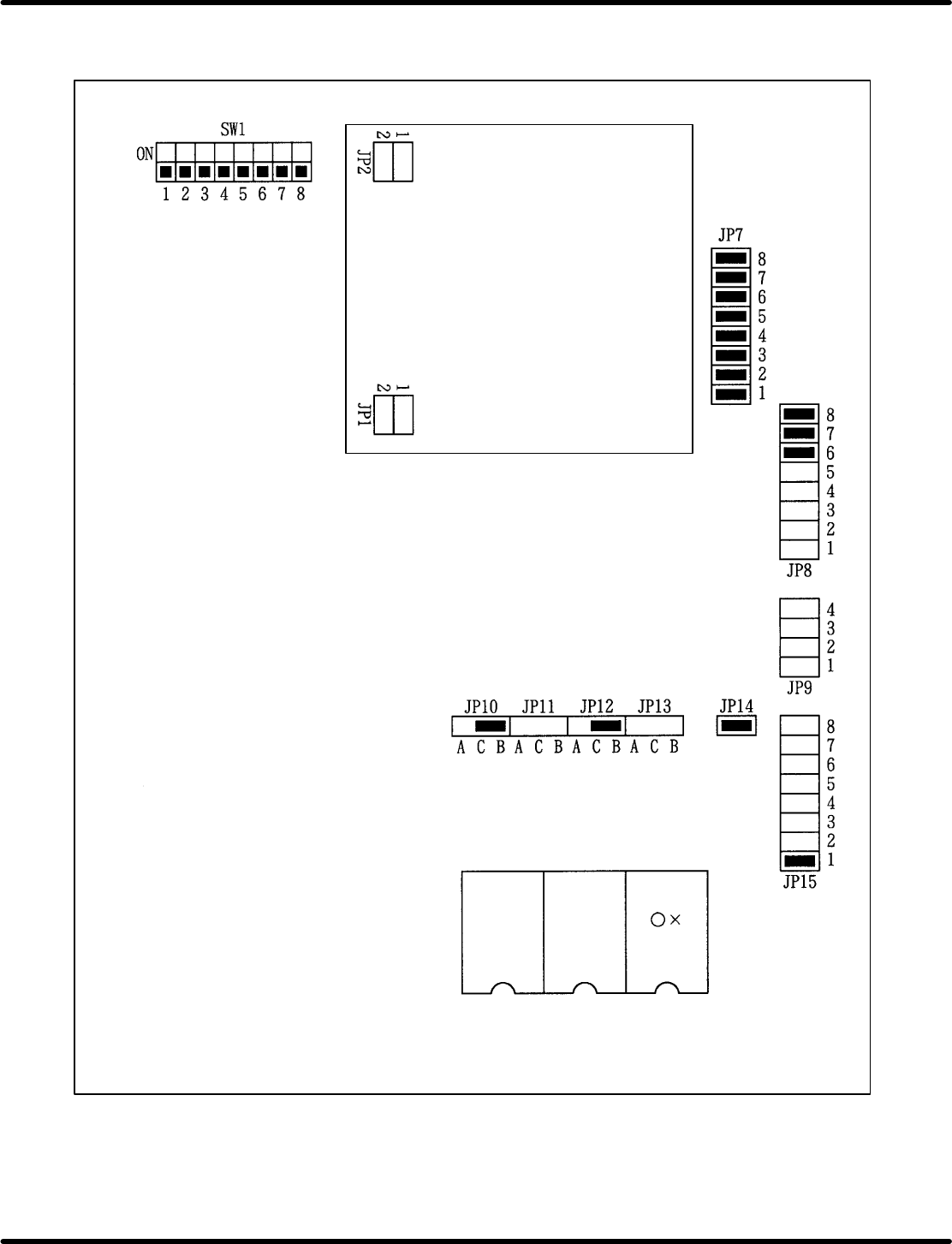
8.3.5 SEQ−SE (I) Board Setting
DST−S board
Firmware
H
Firmware
L

RH5
8.3 List of Jumper Switch Settings
SERVICE MANUAL
8.3−32
DA3SEC−85−540−B0
SEQ−S (I) main board
JP name Description Short or A−C Open or B−C
JP1 SIO CH4 CTS signal terminal resistance SW 100: terminal *1 No terminal
resistance
JP2 SIO CH4 RXD signal terminal resistance SW 100: terminal *1 No terminal
resistance
JP3 SIO CH3 CTS signal terminal resistance SW 100: terminal *1 No terminal
resistance
JP4 SIO CH3 RXD signal terminal resistance SW 100: terminal *1 No terminal
resistance
JP5−1 SIO CH3 CTS signal connecting selection RTS auto group Connect either
JP5−2 External line *1
JP6−1 SIO CH4 CTS signal connecting selection RTS auto group Connect one or
th
th
JP6−2 External line *1
the other.
JP7−1 General−purpose input D8 bit D8= 1 *1 D8= 0
JP7−2 General−purpose input D9 bit D9= 1 *1 D9= 0
JP7−3 General−purpose input D10 bit D10= 1 *1 D10= 0
JP7−4 General−purpose input D11 bit D11= 1 *1 D11= 0
JP7−5 General−purpose input D12 bit D12= 1 *1 D12= 0
JP7−6 General−purpose input D13 bit D13= 1 *1 D13= 0
JP7−7 General−purpose input D14 bit D14= 1 *1 D14= 0
JP7−8 General−purpose input D15 bit D15= 1 *1 D15= 0
JP8−1 Multibus access address setting MA23*Signal MA23*= 0 MA23*= 1
JP8−2 Multibus access address setting MA22*Signal MA22*= 0 MA22*= 1
JP8−3 Multibus access address setting MA21*Signal MA21*= 0 MA21*= 1
JP8−4 Multibus access address setting MA20*Signal MA20*= 0 MA20*= 1
JP8−5 Multibus access address setting MA19*Signal MA19*= 0 MA19*= 1
JP8−6 Multibus access address setting MA18*Signal MA18*= 0 *1 MA18*= 1
JP8−7 Multibus access address setting MA17*Signal MA17*= 0 *1 MA17*= 1
JP8−8 Multibus access address setting MA16*Signal MA16*= 0 *1 MA16*= 1
JP9−1 Multibus access address setting MA15*Signal MA15*= 0 MA15*= 1
JP9−2 Multibus access address setting MA14*Signal MA14*= 0 MA14*= 1
JP9−3 Multibus access address setting MA13*Signal MA13*= 0 MA13*= 1
JP9−4 Multibus access address setting MA12*Signal MA12*= 0 MA12*= 1
JP10 LCA1 (IC86) data transmission mode setting Data download Serial PROM
transmission *1
JP11 LCA1 (IC86) unit reset Unit reset Normal running *1
JP12 LCA2 (IC87) data transmission mode setting Data download Serial PROM
transmission *1
JP13 LCA2 (IC87) unit reset Unit reset Normal running *1
JP14 System program ROM wait setting 1 wait *1 0 wait