KE2010.Instruction Manual.Ver.2.01,Rev.08.pdf - 第148页
4 – 41 (6) Scale type 1) Gr ay scale (Multi-level) recognition Obt ain the level distribution o f the brightness of the mark s in depth and width. Then, calculat e shape of t he mark s and positions of the centers. Becau…
4 – 40
(4) BOC type
To place a component more precisely, positioning marks may be made on a
board.
Select a BOC type according to the actual positioning mark setting.
1) Not used
Production is carried out without using the BOC mark. (The mark printed on
the PWB and to be used for offsetting the placement point.) See Sections
"1.1.7 Printed circuit board specifications" and 5 " Board Recognition Marks
".
2) PWB mark is used
A set of BOC marks are used for the placement point offset of the entire
PWB area. When the BOC mark is used for a single pattern PWB, select
this item. When a set of BOC marks is used for the entire area of a multi
pattern PWB, select also this item.
3) Circuit mark is used
For a multiple pattern PWB, when the BOC mark of each pattern is used for
the placement point offset of each circuit of the PWB, select this item.
Accuracy of placement is better compared with the placement using the BOC
mark but it takes longer to complete the recognition of all BOC marks.
For a non-matrix multiple pattern PWB, the circuit has to be assigned in 90,
180, 270, or 360 degrees against the reference circuit.
(5) Bad mark type
A bad mark may be made on a multiple pattern board so that no component can
be placed on a defective circuit. To use a bad mark, select the bad mark type
according to the difference of reflection ratio between a bad mark and a board.
1) Not used
Select this item when production is carried out without using bad marks.
(The bad marks are used for recognizing a certain circuit of a multiple pattern
PWB where components are not to be mounted. Normally, sealing or
painting is applied for the bad marks.) For a single pattern PWB, the bad
marks cannot be used, and select this item.
2) Mark is light
Select this item when a bad mark and the PWB are recognized with the bad
mark sensor, and the reflection ratio of the bad mark is higher than that of the
PWB.
3) Mark is dark
Select this item when a bad mark and the PWB are recognized with the bad
mark sensor, and the reflection ratio of the bad mark is lower than that of the
PWB. This item shall be selected particularly when black bad marks are
used on a ceramic board.
4 – 41
(6) Scale type
1) Gray scale (Multi-level) recognition
Obtain the level distribution of the brightness of the marks in depth and width.
Then, calculate shape of the marks and positions of the centers. Because
mark recognition is performed using the data obtained from multiple marks,
precise recognition is possible. Normally, select this item.
2) Binary scale (Bi-level) recognition
Obtain the edges of the marks, and calculate shape of the marks and
positions of the centers. Select this item only for the marks those where
multi-level recognition is impossible.
4 – 42
4.5.2 Dimension set up
When you click the <Dimensions> button on the Basic setting window, the system
switches a window to the "Dimensions" window. The settings of the items"Circuit"
and "BOC mk pos" vary depending on the "PWB configuration" setting on the Basic
setting window: Single PWB, Matrix circuit or Non-matrix circuit.
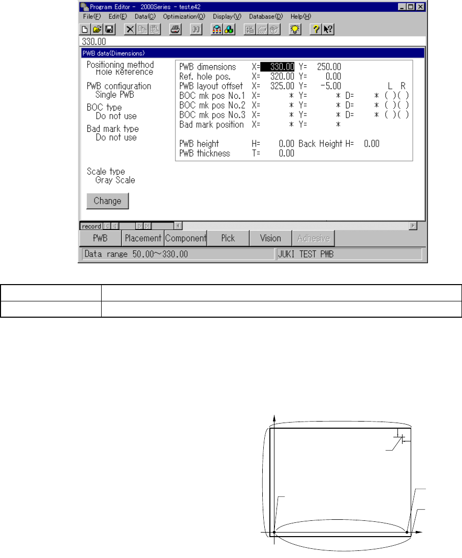
4.5.2.1 Single pattern
When you select “Single PWB” as the PWB configuration and click the <Dimension>
button, a screen shown below appears.
Button Description
Change Displays the Basic setup change screen.
Before entering each dimension on the "Dimensions" column, be sure to set the
origin of each dimension. Since Placement data is created based on this origin, we
recommend that you specify the origin used in CAD data if you are to create
Placement data from CAD data.
① PWB dimensions
Enter the outer dimensions of a
PWB.
X indicates the same direction as
the board transport direction, while
Y indicates the direction
perpendicular to the board
transport direction.
X = 330.00 Y = 250.00
250
330
(320, 0)
(325, -5)
10
10
BOC mark
PWB reference
position (origin)
Reference pin
PWB layout
end point