KE2010.Instruction Manual.Ver.2.01,Rev.08.pdf - 第157页
4 – 50 0 ° (165, 0) (320, 240) 180 ° (155, 240) 180 ° ⑥ BO C mk pos (mar k position) No. 1 to No. 3 W hen y ou select "PWB mark used" as the BOC type on the Basic setup window , enter the dist ance fr om the PW…
4 – 49
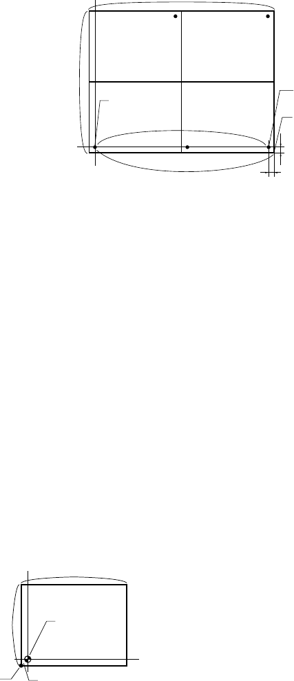
① PWB dimensions
Enter the outer dimensions of a
PWB in the same manner as when
you select “Single PWB” as the
PWB configuration.
X indicates the same direction as
the board transport direction, while
Y indicates the direction
perpendicular to the board
transport direction.
X = 330.00 Y = 250.00
② Ref. hole pos. (Reference hole position)
Enter the coordinates of the positioning hole viewed from the PWB reference
position in the same manner as when you select メ Single PWB モ as the PWB
configuration. These coordinates should be entered with assuming that the
PWB reference position is the origin (0, 0).
Note that the reference hole position varies according to the board transport
direction or reference side: front or rear (see Figure 4.5.2.1). When you
select "Shape Reference" at the item "Positioning method" on the Basic setting
window, you do not have to enter any data here.
X = 320.00 Y = 0.00
③ PWB layout offset
Enter the coordinates of the PWB layout end point viewed from the PWB
reference position in the same manner as when you select "Single PWB" as the
PWB configuration.
Note that the PWB layout end point varies according to the board transport
direction and/or board transport reference side
X = 325.00 Y = - 5.00
165
125
④ Circuit dim. (dimensions)
Enter the outer dimensions of a circuit.
X indicates the same direction as the board transport direction, while Y
indicates the direction perpendicular to the board transport direction. Enter the
dimensions obtained when the "Rot." (rotation) of the Circuit layout is 0 degrees.
X = 165.00 Y = 125.00
⑤ Ckt. (Circuit) layout offset
Enter the coordinates of the circuit layout end point viewed from the circuit
reference position.
The circuit layout end point is fixed at the lower left corner of the circuit.
X = - 5.00 Y = - 5.00
Circuit reference position (0, 0)
Circuit layout end point Circuit layout offset (-5, -5)
250
330
(320, 0)
(325, -5)
5
PWB reference
position (0, 0
)
Reference pin
PWB layout
end
p
oint
4 – 50
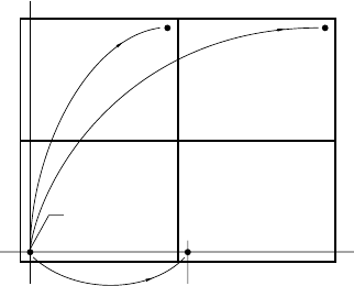
0°
(165, 0)
(320, 240)
180°
(155, 240)
180°
⑥ BOC mk pos (mark position) No. 1 to No. 3
When you select "PWB mark used" as the BOC type on the Basic setup window,
enter the distance from the PWB reference position to the center point of the
BOC mark.
When you select "Ckt. mark is used" as the BOC type on the Basic setup
window, enter the distance from the circuit reference position to the center point
of the BOC mark. Note that each BOC mark position should be entered which
is obtained when the "Rot." (rotation) of the "Circuit layout" is 0 degrees.
You can select two or three BOC marks. When you use three BOC marks, you
can use any of three BOC marks.
When using two BOC marks, select the two BOC marks which are placed
diagonally on the PWB. The position of the BOC mark can be taught.
An asterisk mark (*) in the parentheses is used to indicate the data completion
status.
For a user-designated template, "T" appears in the parentheses after the
system teaches the right station (see Section 5.4 "Teaching a Mark").
⑦ Bad mark position
Enter the bad mark position viewed from the circuit reference position.
Enter the dimensions obtained when the "Rot." (rotation) of the Circuit layout is
0 degrees. A bad mark can be taught also.
See Section 7.2.2.15 " Bad mark sensor teaching ".
⑧ PWB height
If the height of the side on which a component is to be placed when a board is
clamped with a jig or like is different from that obtained when a flat board is
clamped, enter the difference with assuming that the height of the clamped flat
board upper side is 0.
The "+" sign indicates the up direction, while the "" sign does the down direction.
Since you cannot set the height of a board for each circuit, the height of each
circuit should be the same if you are to create a jig.
Normally, set this item to "0.00".
⑨ PWB thickness
Enter the thickness of a PWB in the same manner as when you select “Single
PWB” as the PWB configuration.
The support plate moves up according to the thickness of a PWB entered here
to support the PWB.
Circuit layout
4 – 51
⑩ Back Height
Enter the distance from the board transfer reference side to the bottom side of a
PWB including components (note that any component located on the bottom of
a PWB should not interfere with the support table).
The value you entered here is used as the support plate waiting position during
production.
The shorter the support plate moves, the shorter the board transport cycle time
becomes.
⑪ Circuit layout
When you click the <Ckt. lyt> button, the "Circuit layout" window, which allows
you to enter the circuit layout data, opens. Use the up, down, left and/or right
cursor keys or a track ball to move the cursor, then enter a numeric character.
Enter to the "X" and "Y" columns the distance from the origin of the board to
that of each circuit. Enter to the "Rot." column the angle of each circuit with
assuming that the circuit on which Placement data is created based is located
at 0 degrees and the anti-clockwise direction is positive. After entering data,
click the [Exit] command to return to the "Dimensions" window.
Note: When you select “PWB mark used” as the “BOC type” on the PWB data basic
setting screen, enter a multiple of 90 degrees to the “Rot.” cell.
No.1
No.2
No.4
No.5
No.3
Y5Y1
Y3
Y4Y2
X1
X2
X3
X4
X5
Origin of a board
Origin of a circuit
Component