Omron V-TS Teaching Manual.pdf.pdf - 第124页
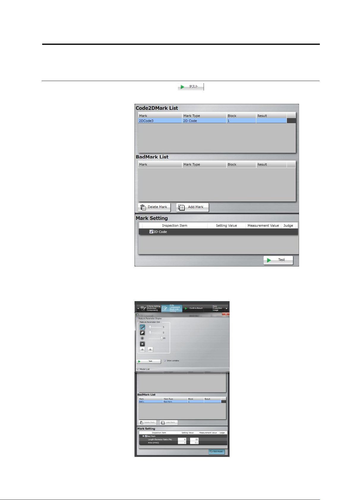
2.7 PCB/Com ponent Block Unit Setting 2- 97 6. By clicking the button, the test result of the 2D c ode, measured value, and ju dgm ent are displayed. 7. W hen setting a bad mark, select the check box of the inspection it…
Chapter 2 Inspection Programming
2-96
3.
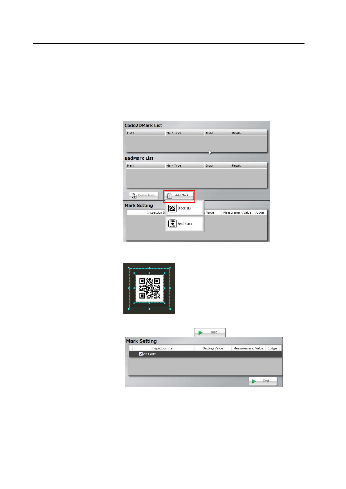
Select the target (PCB or Component Block Unit) of adding a mark
on the PCB Layout list. Click [Add Mark] and select a mark type in
the mark list.
Selectable mark types are as follows:
When selecting a PCB: PCB ID
When selecting a component block unit: Block ID or Bad Mark
4.
Drag and drop the cursor to surround the mark (2D code/bad mark)
in the image display area.
5.
On the mark setting screen, select a checkbox on the inspection
item column, and click the button.

Chapter 2 Inspection Programming
2-98
8.
Click the button. The result of the bad mark,
measured values, and judgment are displayed.
The display of the inspection result of PCB tests is switched
depending on whether a bad mark is detected or not.
- If detected: The inspection result of all the circuits of the
component block units to which the bad mark belongs is not
displayed.
- If not detected: The inspection result of the circuits is
displayed.