Omron V-TS Teaching Manual.pdf.pdf - 第231页
Chapter 2 Insp ection Progr amming 2- 204 ⑦ Overlay Switch: T he extracted pixels on the PCB su rface (c yan c olor portion) ar e displayed. ⑧ Displa y Magnification Slider: Enables to chan ge the m agnification of displ…
2.16 Managing PCB Images
2-203
■Position Correction Model Editing Tool: Explanation of Screen Functions
This section explains various functions displayed on the right side of the Reference Level
Model Editing Tool .
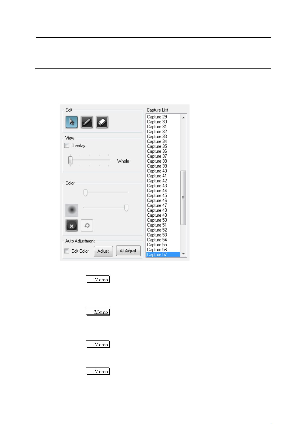
①Selection Button: Use when selecting a land on the screen. For the selected land, position
and size can be edited.
It is unable to move the position and size of the land out of the
inspection range window.
②Pen Tool: When a pixel extracted on the PCB surface is clicked, the color of the pixel is
added to the color table. Pen’s thickness can be specified with the slide bar.
Pen's thickness can be specified in a range of one to 21 pixels.
③Eraser Tool: When the extracted pixel on the PCB surface (cyan color portion) is clicked,
the color of the pixel is deleted from the color table. Eraser’s thickness can be specified with
the slide bar.
Eraser’s thickness can be specified in a range of one to 21 pixels.
④Extension Range Setup Tool: Specify the extension range of the color of the pixel selected
by the pen/eraser tool with the slide bar.
The extension range can be specified in a range of 0-20.
⑤Clear Button: All color settings are deleted from the color table.
⑥Undo Button: Edited content of the color table can be cancelled.
⑧
①
②
③
④
⑤
⑥
⑦
⑨
⑩
⑪
⑫
Chapter 2 Inspection Programming
2-204
⑦Overlay Switch: The extracted pixels on the PCB surface (cyan color portion) are
displayed.
⑧Display Magnification Slider: Enables to change the magnification of display.
⑨Capture List: The visual field of the inspection program is displayed.
⑩Edit Color Switch: A color table to adjust the land position automatically can be displayed/
edited.
⑪Adjust Button: The position of the selected land window is adjusted automatically.
⑫All Adjust Button: The positions of all the land windows are adjusted automatically.
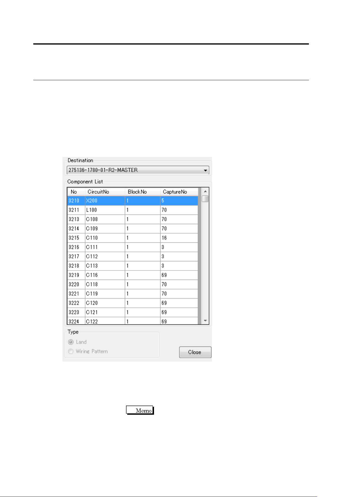
⑬Destination Button: If destinations are set, the destinations edited can be changed.
⑭Component List: Component numbers, circuit numbers, component block unit numbers,
and affiliated inspection visual field numbers are displayed. When a line is selected, control
is moved to the component and a window is displayed.
⑮Type: The reference of the position correction model can be changed.
If post-mounting inspection is conducted and it is detected that
solder paste extends beyond the land, or if a lot of bottom
electrode components such as BGA are implemented and the
land is not visible, select [Wiring Pattern].
⑯Close Button: The position correction model which has been edited completely is saved.
⑬
⑭
⑮
⑯
2.16 Managing PCB Images
2-205
削除: Managing PCB Images
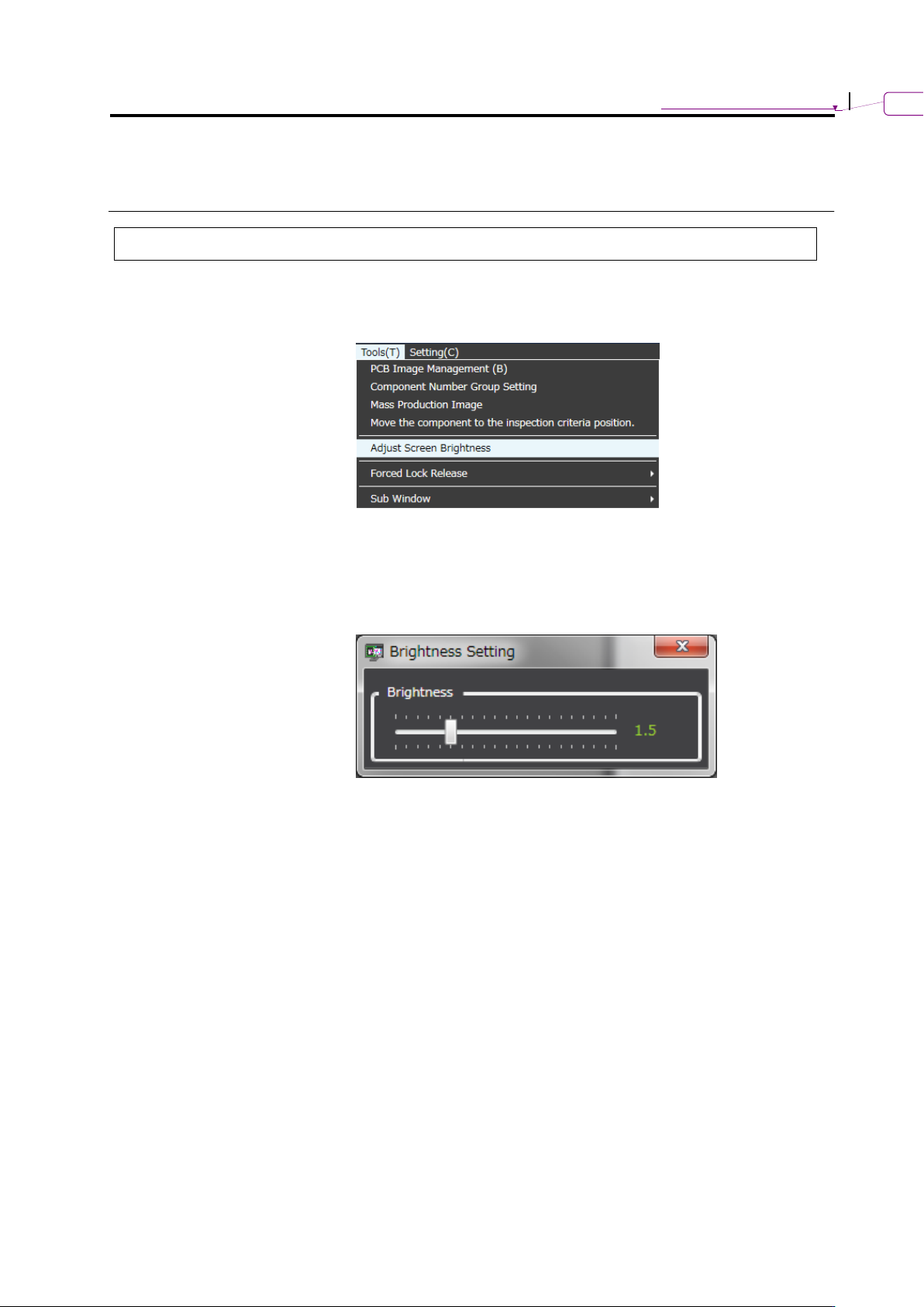
2.16.6 Changing Brightness of PCB Image
You can change brightness of a PCB image currently displayed.
1.
On the menu bar of the edit screen, select [Tool] - [Adjust screen
brightness].
2.
On the [Brightness Setting] dialog box, move the slider right/left to
adjust the brightness. To adjust screen brightness, use the
[Brightness] slider.
The initial value has a brightness of 1.5.
3.
After adjustment, close the dialog box.