Omron V-TS Teaching Manual.pdf.pdf - 第65页
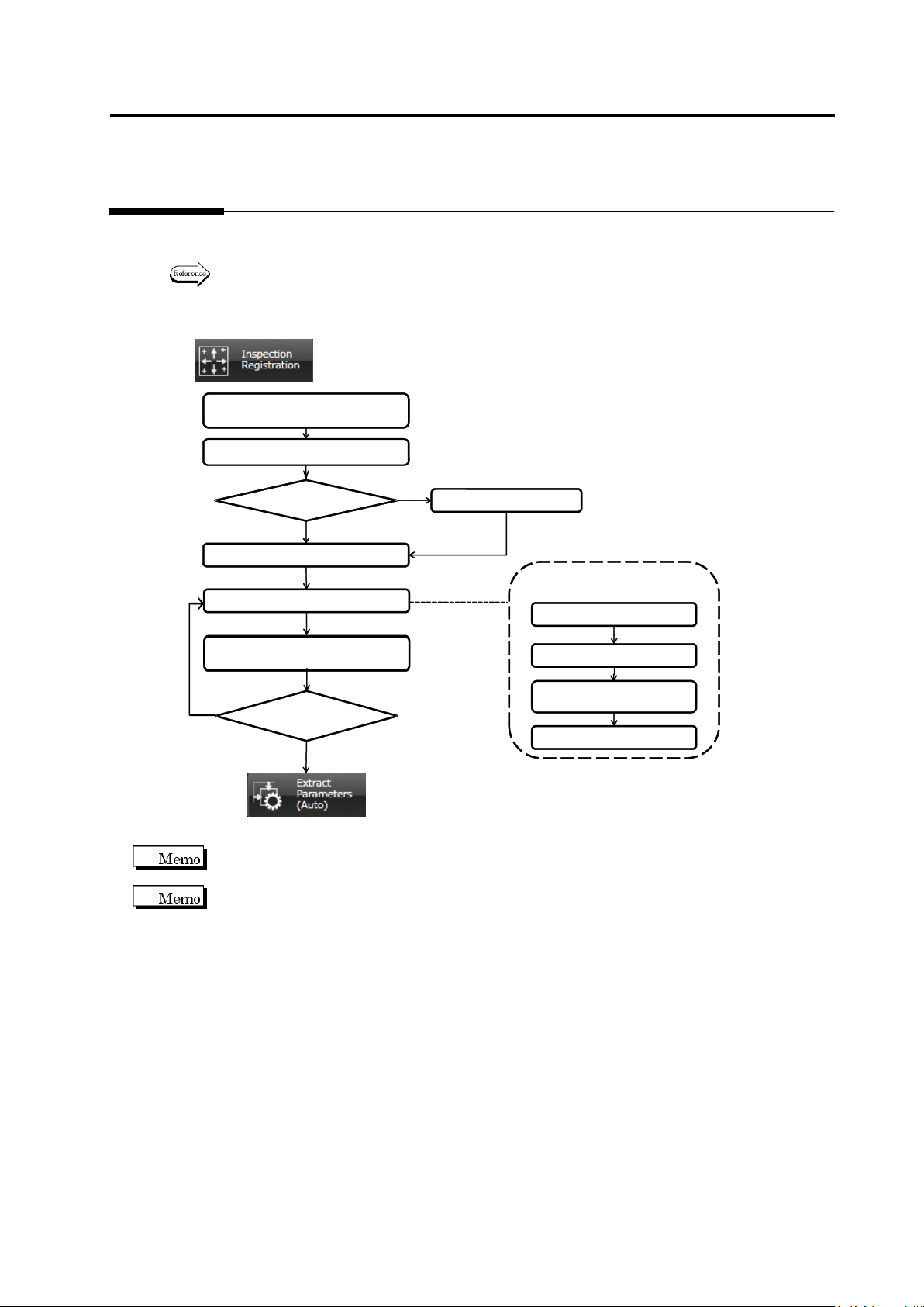
Chapter 2 Inspecti on Programm ing 2- 38 2.4.1 Regis tering Position Adj ustment Marks Register PCB position adjustment m arks. Registering them provides m ore precise adjustm ent of inspection windows durin g PCB inspec…
2.4 Registering for Inspection
2-37
2.4 Registering for Inspection
This section details the operation required in the Inspection Registration screen.
Position inspection windows on the component following the procedures below.
Refer to the individual section described in the flow chart for details of each procedure.
2.4.1 Registering Position
Adjustment Marks
2.4.4 Inspection Registration
2.4.5 Component Registration
2.4.2 Selecting Mount Data
2.4.3 Mount Alignment
All Component Numbers
Registered?
Yes
No
Operation Flow in (2.4 Registering for Inspection)
2.4.5.1. Component Setting
2.4.5.4. Electrode Setting
2.4.5.2. Land Setting
2.4.5.3. Electrode Group
Setting
2.4.5 Component
Registration Detailed Flow
Mount Data
Selected?
Yes
No
(2.4.6 Setting Component
Number Group)
(2.5 Registering the Component
Number Model)
Clicking [Next] at the bottom of the screen switches the screen displays in the order shown in the
flow chart, and [Back] switches them in the reverse order.
The Inspection Registration screen (See 2.4.4 “Inspection Registration”) appears as the initial
screen if an inspection program with the mount data loaded is opened.
Chapter 2 Inspection Programming
2-38
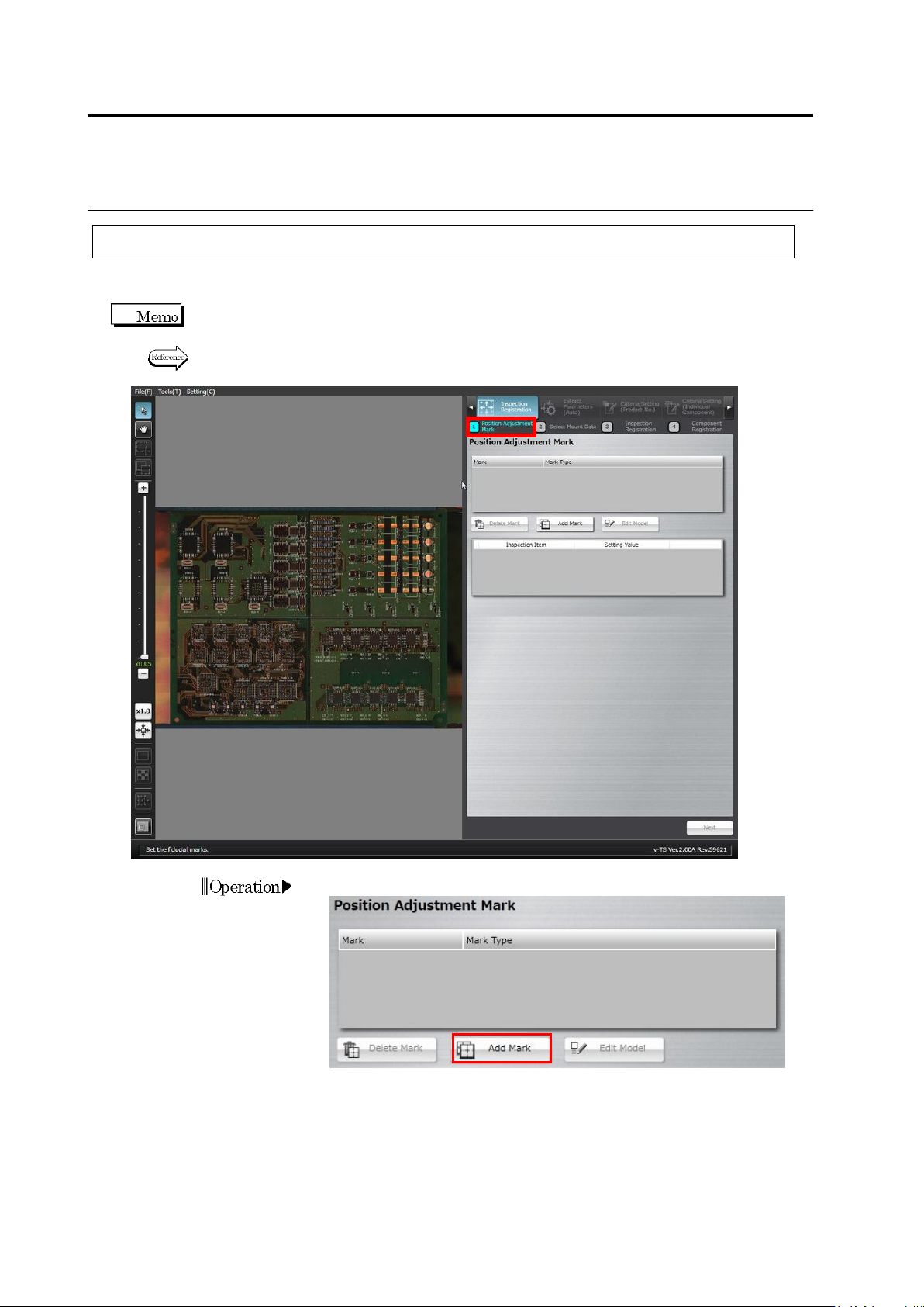
2.4.1 Registering Position Adjustment Marks
Register PCB position adjustment marks. Registering them provides more precise adjustment of
inspection windows during PCB inspection.
Two PCB adjustment marks must be set. Those at the ends of a diagonal line of the PCB are
normally selected.
Refer to the Inspection Logic Manual, "2.2 Fiducial Adjustment" for the details on PCB position
adjustment.
1.
Click [Add Mark].
Operation
2.4 Registering for Inspection
2-39
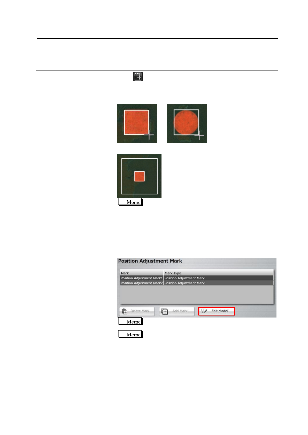
2.
Click (Create Window) button in the Image Operation tool bar.
Drag the mouse cursor to a corner of the PCB to surround the
adjustment marks.
Square Mark Circular Mark
Drop the cursor. The mark detection area is automatically drawn.
The size of individual windows can be adjusted.
The minimum and maximum values of the outer window are as
follows:
Minimum: 2.4 x 2.4mm
Maximum: visual field’s size (different for each model)
3.
Repeat Steps 1 and 2 for the mark at the diagonally opposite corner
of the PCB.
4.
Click [Edit Model].
The [Edit Model] button becomes effective after two
adjustment marks are registered.
When you select the position adjustment mark, the [Delete
Mark] button becomes enabled.