Omron V-TS Teaching Manual.pdf.pdf - 第297页
Appendix 7. Positio n Correction/Extractio n a- 20 Example 2: V erif ying extraction offset of QFP On the left and center figur es the distrib ution widths are within 20 % so they are ju dged as no offset. On the right f…
Appendix 7. Position Correction/Extraction
a-19
3. Extraction offset confirmation procedure
After conducting a PCB test using an adjustment image, whether the extraction offset occurs or not on
the component number (component number group) in which an inspection fault has occurred is verified
based on the shape of the histogram of the model editing screen according to the following inspection
items.
When the extraction offset occurs, refer to the component extraction procedure and the
component tip extraction procedure of appendix section 5 and 7, respectively to adjust to
eliminate extraction offset.
Comp. type
Condition
Inspection item to select
Judgment criteria for no
skew
Chip component
Electrode
capacitor
Transistor
Powered
transistor
2-pin mini mold
Non-lead
component
Other component
applicable to the
conditions on the
right
Component whose
width is at least 120%
or no electrode for the
electrode width
For the component body
window:
- Component offset –
Offset X [Absolute
value]
- Component offset –
Offset Y [Absolute
value]
All the measured
values of good
components must be
within the default
inspection criteria.
IC
Connector
Resistor array
The width of the land
for the electrode width
is less than 120%.
Electrode window:
- Side overhang
- End overhang
The distribution width of
the measured value of
the good component
must be 20% or less.
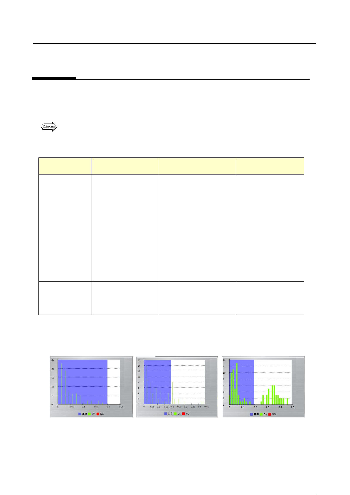
Example 1: Verifying extraction offset of 2-pin mini mold
On the left figure, the values are within the inspection criteria so it is judged as no offset. On the center
and right figures the values are not within the inspection criteria so they are judged as offset.
Appendix 7. Position Correction/Extraction
a-20
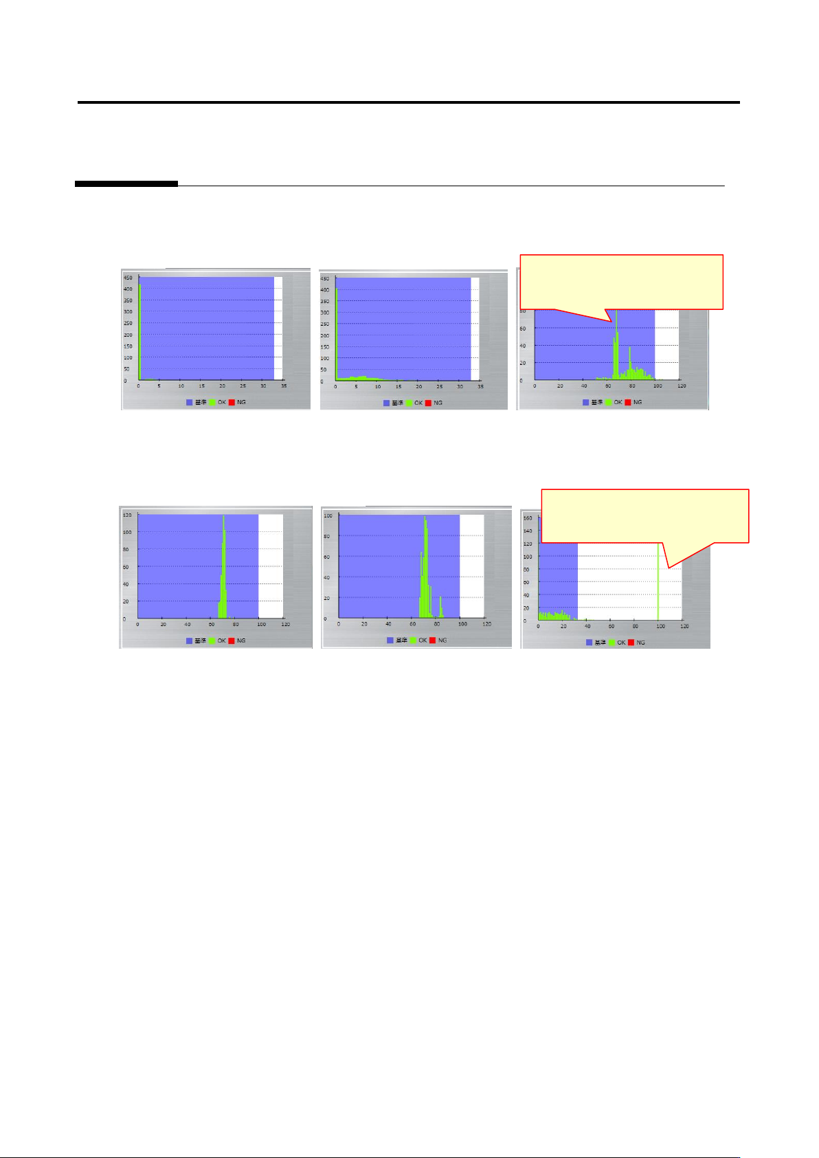
Example 2: Verifying extraction offset of QFP
On the left and center figures the distribution widths are within 20% so they are judged as no offset. On
the right figure the distribution width is larger than 20% so it is judged as an offset.
Example 3: Verifying extraction offset of QFP
On the left and center figures the distribution widths are within 20% so they are judged as no offset. On
the right figure the distribution width is larger than 20% so it is judged as an offset.
The minimum and maximum values
are 0% and 100% respectively, and the
distribution width is 100%, making it
larger than 20%.
The minimum and maximum values
are 49% and 106% respectively, and
the distribution width is 57%, making it
larger than 20%.
Appendix 7. Position Correction/Extraction
a-21
4. Inspection items adjustable with characteristic parameters
When false call or detection failure occurs and the characteristic parameters regarding the inspection
items can be adjusted, characteristic parameters should be adjusted.
1) For a false call, adjust that the measurement value of the good component is within the inspection
criteria.
2) For a detection failure, adjust that the good and fault can be separated using the histogram.
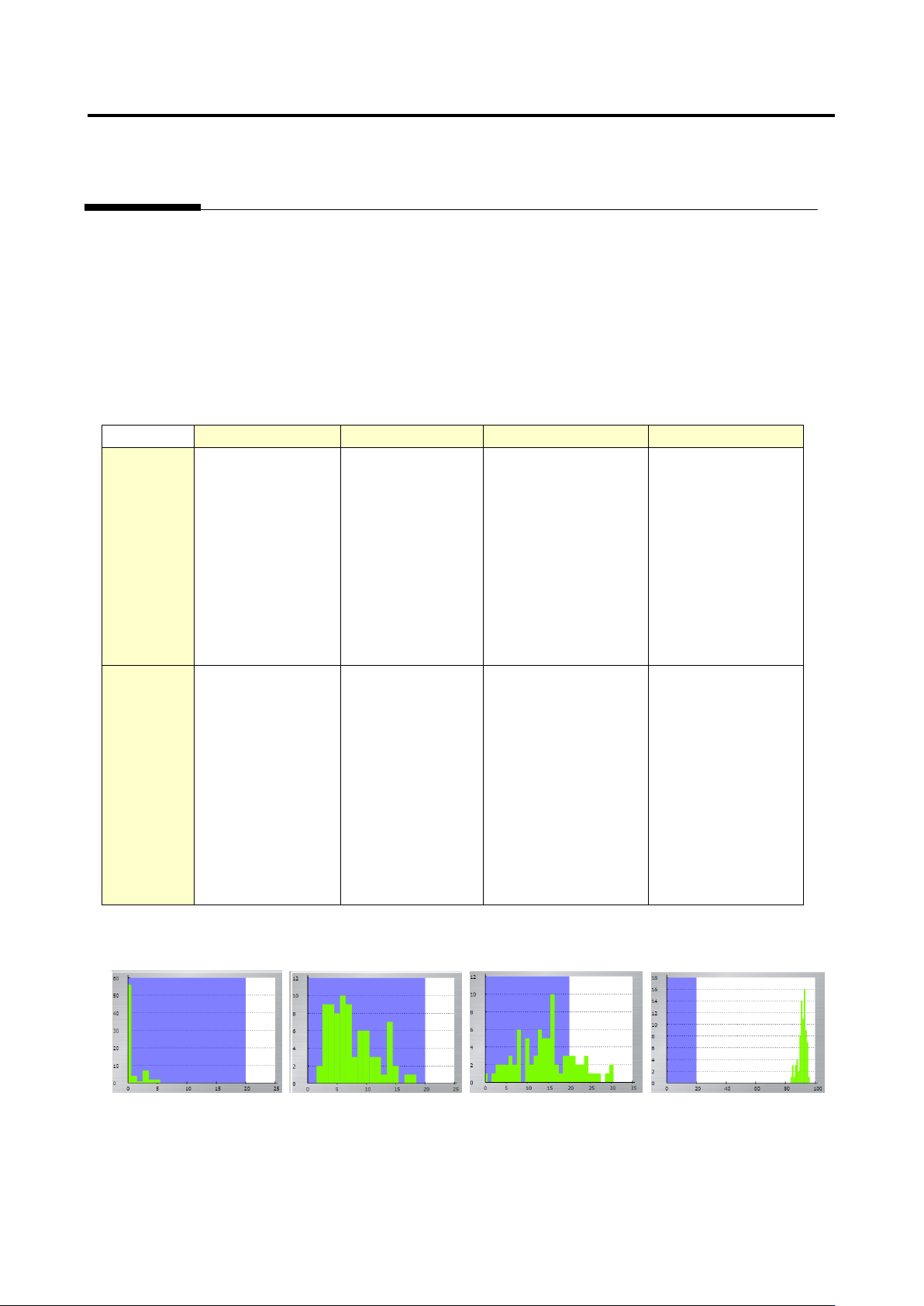
* Adjust the good component so that the value is within the inspection criteria, as shown in (1).
Component
Electrode
Land
Inspection range
Adjustable
Missing
component
Component
difference
Polarity difference
Upside down
component
X position gap
Y position gap
Component skew
Side overhang
End overhang
End overlap
Electrode length
Electrode area
Side bend
Electrode height
(oblique)
Exposed land
Land error
Foreign object (land)
Exposed land
(oblique)
Solder ball
Solder bridging
Foreign object
Solder ball (oblique)
Solder bridging
(oblique)
Not
adjustable
None
Exposed
electrode tip
(oblique)
Electrode color
deviation
Exposed
electrode tip
(oblique)
Electrode color
deviation
(oblique)
Fillet inspection (all)
None
In the two figures on the left, the values are within the inspection criteria, and in the two figures on the
right, the values are not within the inspection criteria.