Omron V-TS Teaching Manual.pdf.pdf - 第229页
Chapter 2 Insp ection Progr amming 2- 202 2.16.5 Editing a Pos ition Correction Mod el W hen conducting inspection on the machine or test ing PCBs using v- TS , if the land extraction position is diff erent from that of …
2.16 Managing PCB Images
2-201
<Curved face approximation setup function>
Use this function when the base plane in the inspection image cannot be approximated to a
plane due to distortion of the base plane such as a flexible PCB.
Use the ㉒ base plane approximation method selecting combo box to set this function as
curved face approximation (quadric).
For the settings of base plane, refer to “Curved Face Approximation of Base Plane” of
Section 2.4 “Base Plane Setup” in the inspection logic manual.
<Base plane per-component partitioning function>
This function partitions a base plane on a component basis and sets the partitioned ones
automatically.
Use this function if the height of base planes does not become equal to each other even after
using the ⑮ base plane per-block partitioning function or the ㉒ curved face approximation
setup function. By clicking the ⑯ Component button, the base plane is partitioned in the overall
FOV on a component basis.
To use this function, it is assumed that component block unit has been set up.
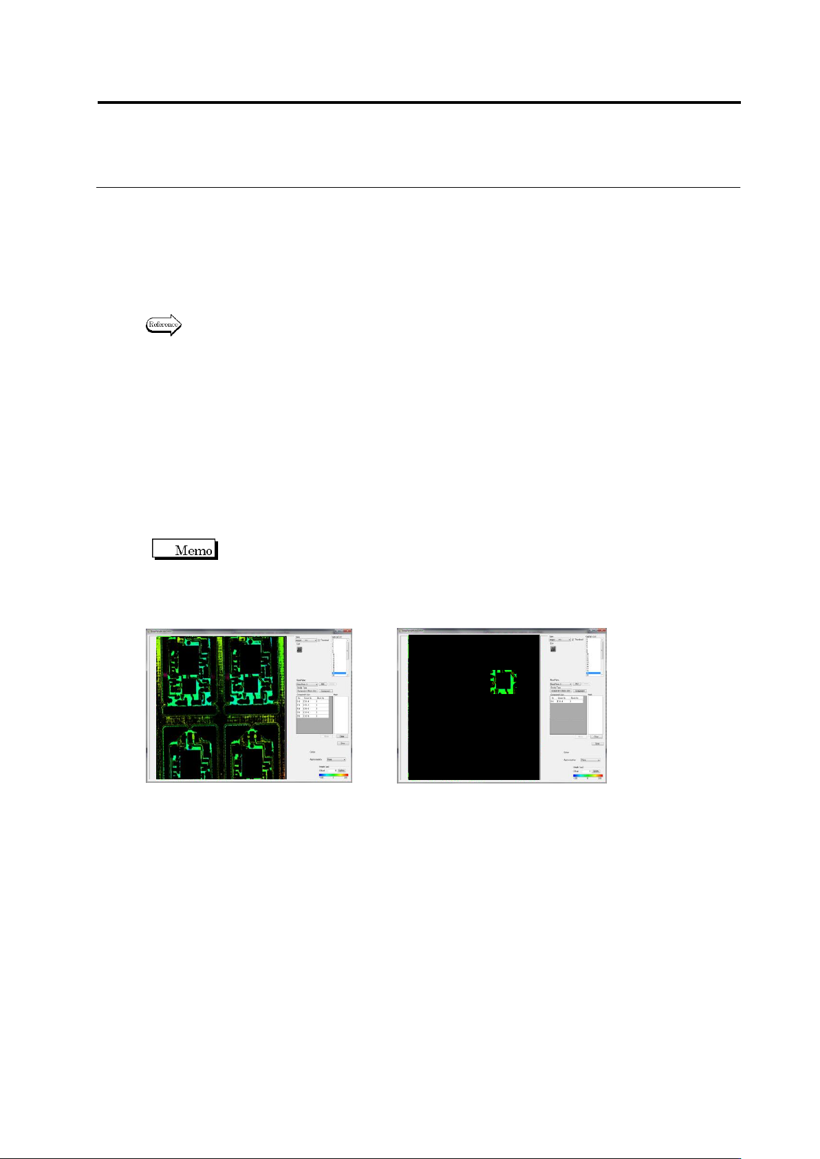
Hereafter the effect of this function is shown.
Before setup After setup
4.
Finish editing of the reference level model. To save the edited data,
click the
㉑
Save button, and click the Close (x) button in the upper
right corner of the window to return to the base plane management
image screen.
Chapter 2 Inspection Programming
2-202
2.16.5 Editing a Position Correction Model
When conducting inspection on the machine or testing PCBs using v-TS, if the land extraction
position is different from that of the actual PCB, edit the position correction model using the
position correction model editing tool. This section describes the operation procedure of this tool.
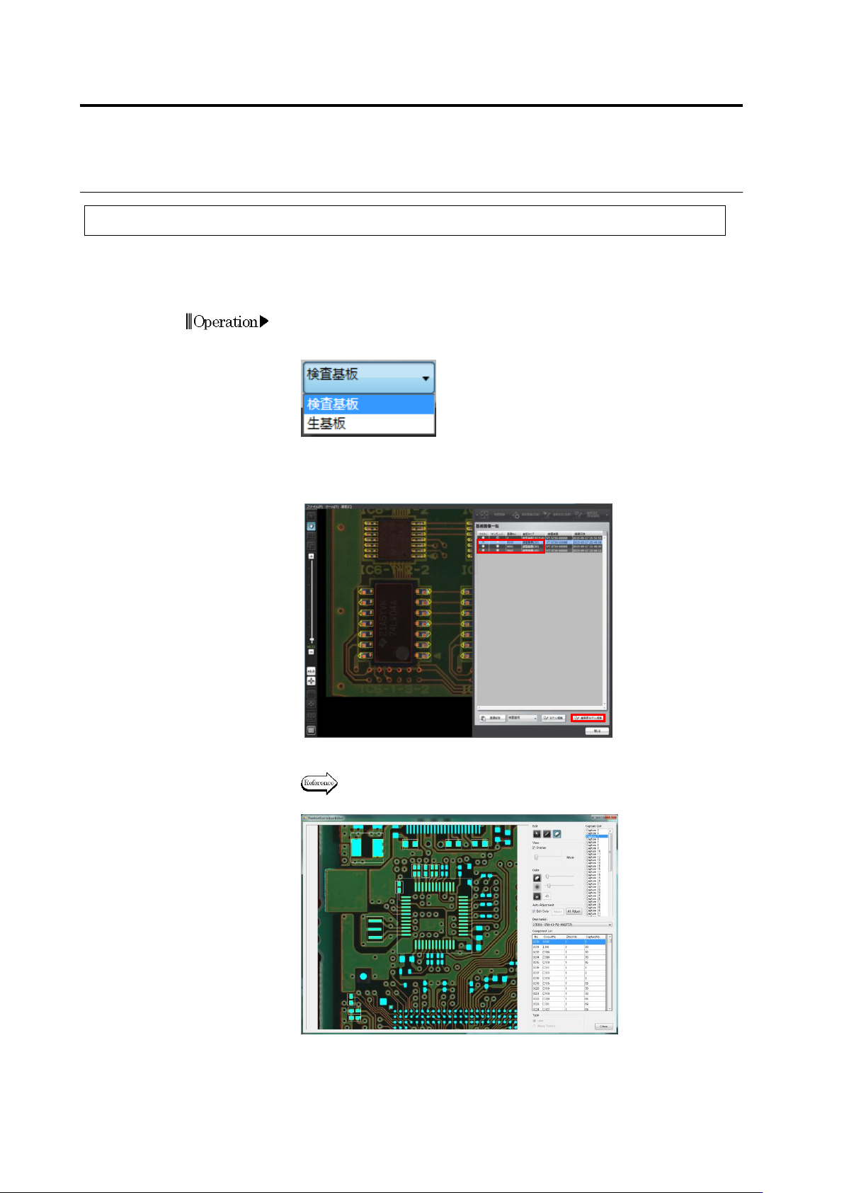
1.
On the menu bar of the editing screen, select [Tool] - [PCB Screen
Management Screen]. If a raw PCB screen is displayed, select
“Inspection PCB” from the list.
2.
On the PCB screen list, click the inspection PCB image edited
(PCB type: adjustment image) to select it to a master. Then, click
[Edit Reference Level Model] to start up the reference level model.
3.
Edit the position correction model.
The editing method using the position correction model
editing tool is described on and after the next page.
2.16 Managing PCB Images
2-203
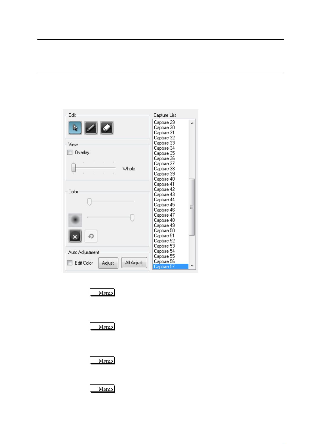
■Position Correction Model Editing Tool: Explanation of Screen Functions
This section explains various functions displayed on the right side of the Reference Level
Model Editing Tool .
①Selection Button: Use when selecting a land on the screen. For the selected land, position
and size can be edited.
It is unable to move the position and size of the land out of the
inspection range window.
②Pen Tool: When a pixel extracted on the PCB surface is clicked, the color of the pixel is
added to the color table. Pen’s thickness can be specified with the slide bar.
Pen's thickness can be specified in a range of one to 21 pixels.
③Eraser Tool: When the extracted pixel on the PCB surface (cyan color portion) is clicked,
the color of the pixel is deleted from the color table. Eraser’s thickness can be specified with
the slide bar.
Eraser’s thickness can be specified in a range of one to 21 pixels.
④Extension Range Setup Tool: Specify the extension range of the color of the pixel selected
by the pen/eraser tool with the slide bar.
The extension range can be specified in a range of 0-20.
⑤Clear Button: All color settings are deleted from the color table.
⑥Undo Button: Edited content of the color table can be cancelled.
⑧
①
②
③
④
⑤
⑥
⑦
⑨
⑩
⑪
⑫