Omron V-TS Teaching Manual.pdf.pdf - 第214页
2.16 M anaging PC B Im ages 2- 187 2.16 Managing PCB Images The PCB Image M anagement scr een is provided for t he deletion of PCB images and m odel editing of position corr ection colors, solder co lors, land exposure c…
Chapter 2 Inspection Programming
2-186
4.
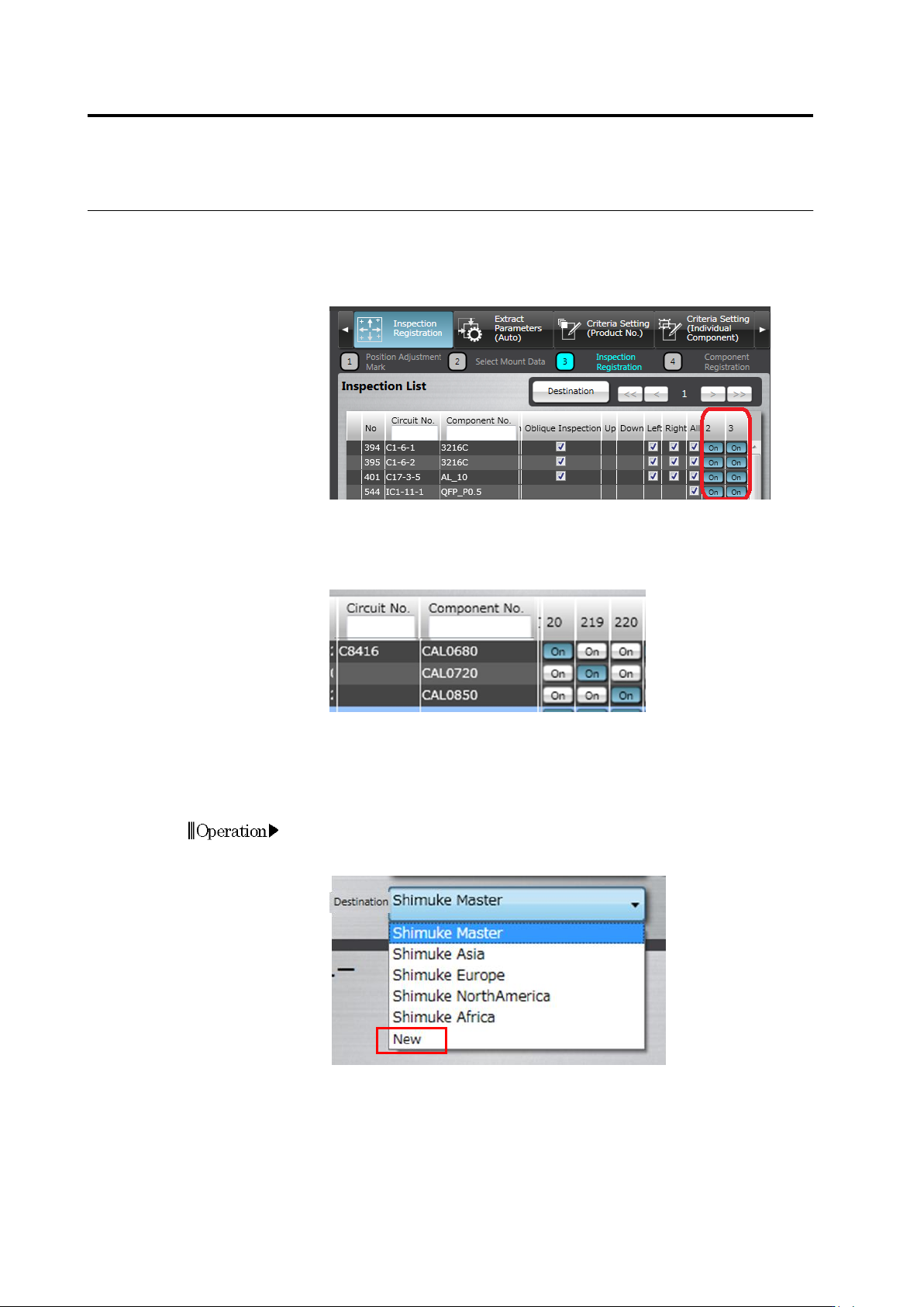
When the [Next] button is clicked, software operates as follows:
If the component is included in the mount data, the [ON] button is
set ON for the component number included in each destination on
the list. If the component is not included in the mount data, the [ON]
button is set OFF.
5.
To add component numbers to a circuit manually as a destination,
select the target circuit, and click [Add Component Number]. For the
component numbers with the same circuit number, the circuit
number is displayed for the first component number only.
Method 2: When there is mount data for each destination:
By this procedure, mount data corresponding to each destination is read in. Then, circuits and
component numbers are set up.
1.
Press the [Return] button to return to the [Select Mount Data]
screen.
2.
Click the [Destination] pull-down menu to select [New].
3.
Read in the mount data to position it.
4.
Execute steps 2 and 3 repeatedly for the number of necessary
destinations.
2.16 Managing PCB Images
2-187
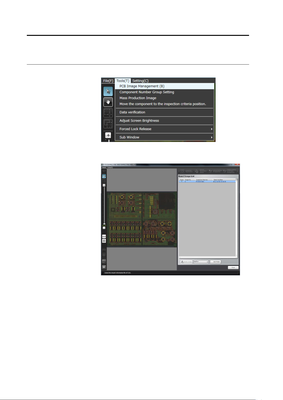
2.16 Managing PCB Images
The PCB Image Management screen is provided for the deletion of PCB images and model
editing of position correction colors, solder colors, land exposure colors, fillet exclusion colors,
and PCB colors.
2.16.1 Accessing the PCB Image Management Screen
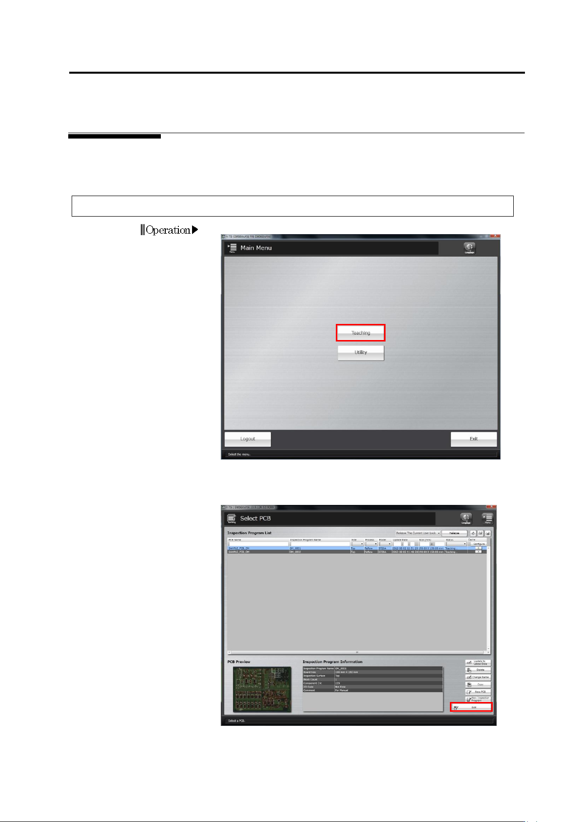
1.
Click [Teaching] in the Main menu.
2.
The Select PCB screen appears.
Select the inspection program to manage the images in the
Inspection Program List, and click [Edit].
Operation
Chapter 2 Inspection Programming
2-188
3.
Select [Tool] - [PCB Image Management] in the editing screen
menu bar.
The PCB Image Management screen is displayed.
Click [Close] to close the PCB image management screen and
return to the inspection program edit screen.