Omron V-TS Teaching Manual.pdf.pdf - 第221页
Chapter 2 Insp ection Progr amming 2- 194 2. Click to select the inspect ion PCB im age (PCB type: adj ustment image) fr om the PCB image list, and click [Edit Reference Level Model]. 3. Edit the reference lev el model. …
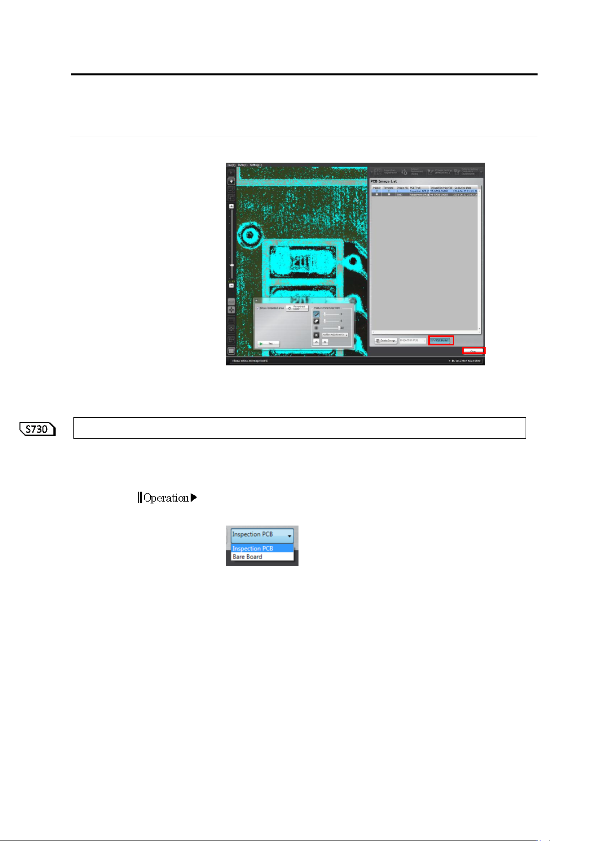
2.16 Managing PCB Images
2-193
5.
Clicking [Edit Model] again closes the color table editing toolbox.
Click [Close]. The Inspection Program Editing screen returns.
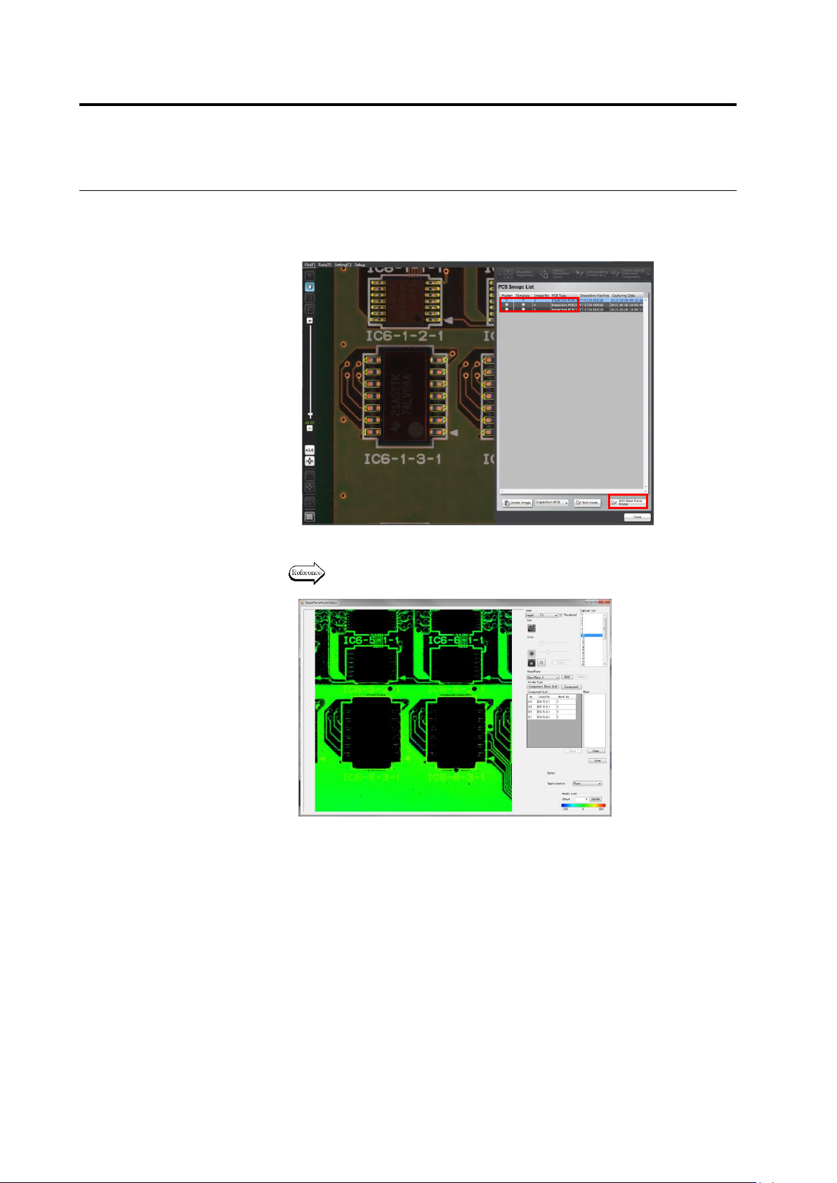
2.16.4 Editing a Reference Level Model
When conducting inspection or v-TS PCB tests by the system, if a measured component height is
different from the height of the real component, use the reference level model editing tool to edit
the reference level model. This section describes the operation procedure of this tool.
1.
On the menu bar of the edit screen, select [Tool] - [PCB Image
Management Screen]. If a bare board image is displayed on the
screen, select Inspection PCB from the list.
Chapter 2 Inspection Programming
2-194
2.
Click to select the inspection PCB image (PCB type: adjustment
image) from the PCB image list, and click [Edit Reference Level
Model].
3.
Edit the reference level model.
The usage of the reference level model editing tool is described in and
after the following page.
2.16 Managing PCB Images
2-195
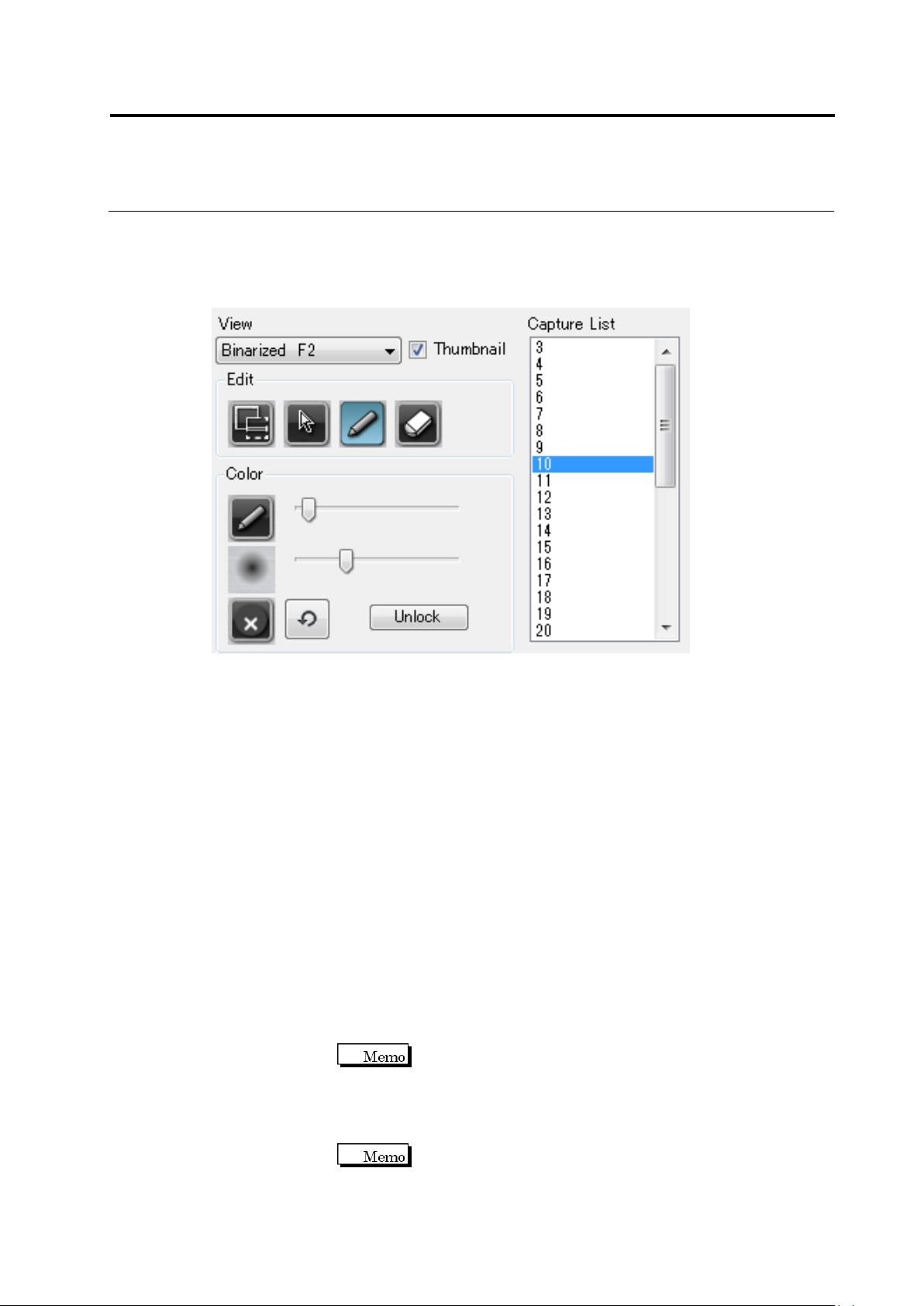
■ Reference level model editing tool - Description on the screen functions
This section describes each function displayed in the right pane of the screen of the
reference level model editing tool.
① View : Image selecting combo box.
Source F1 : Displays the RGB image of the inspection FOV edited.
Binarized F2 : Displays the image binarized from an RGB image by the color table.
Height F3 : Displays the height image of the base plane.
② Thumbnail button : Use this button to display the thumbnail of an inspection FOV
image. The FOV image can be displayed as a thumbnail by turning
ON this button, and in the original FOV size by turning OFF this
button.
③ Inspection FOV list : Displays the FOV of the inspection program.
④ Add mask button : A mask can be added by dragging a target area.
⑤ Select button : Use this button to select various areas on the screen, such as a
component, mask, or base plane.
⑥ Pen tool : By clicking a pixel to be extracted on the PCB, the color of the
pixel is added to the color table. Pen’s thickness can be specified
using the slide bar.
Pen’s thickness can be specified in a range of 1-21 pixels.
⑦ Eraser too : By clicking a pixel to be extracted from the PCB (area colored in
cyan blue), the color of the pixel is deleted from the color table.
Eraser’s thickness can be specified using the slide bar.
Eraser’s thickness can be specified in a range of 1-21
pixels.
①
②
③
④
⑤
⑥
⑧
⑨
⑩
⑦
⑪