Omron V-TS Teaching Manual.pdf.pdf - 第56页
2.2 Creat ing a N ew Inspec tion Program 2- 29 書 式変 更: フォ ント : ( 日 ) MS ゴ シッ ク, 1 0 pt 削除 : Crea ti n g a New In s p e c ti o n P ro g ra m Be careful about the following after setting ON/OFF this function: Since the FOV…
Chapter 2 Inspection Programming
2-28
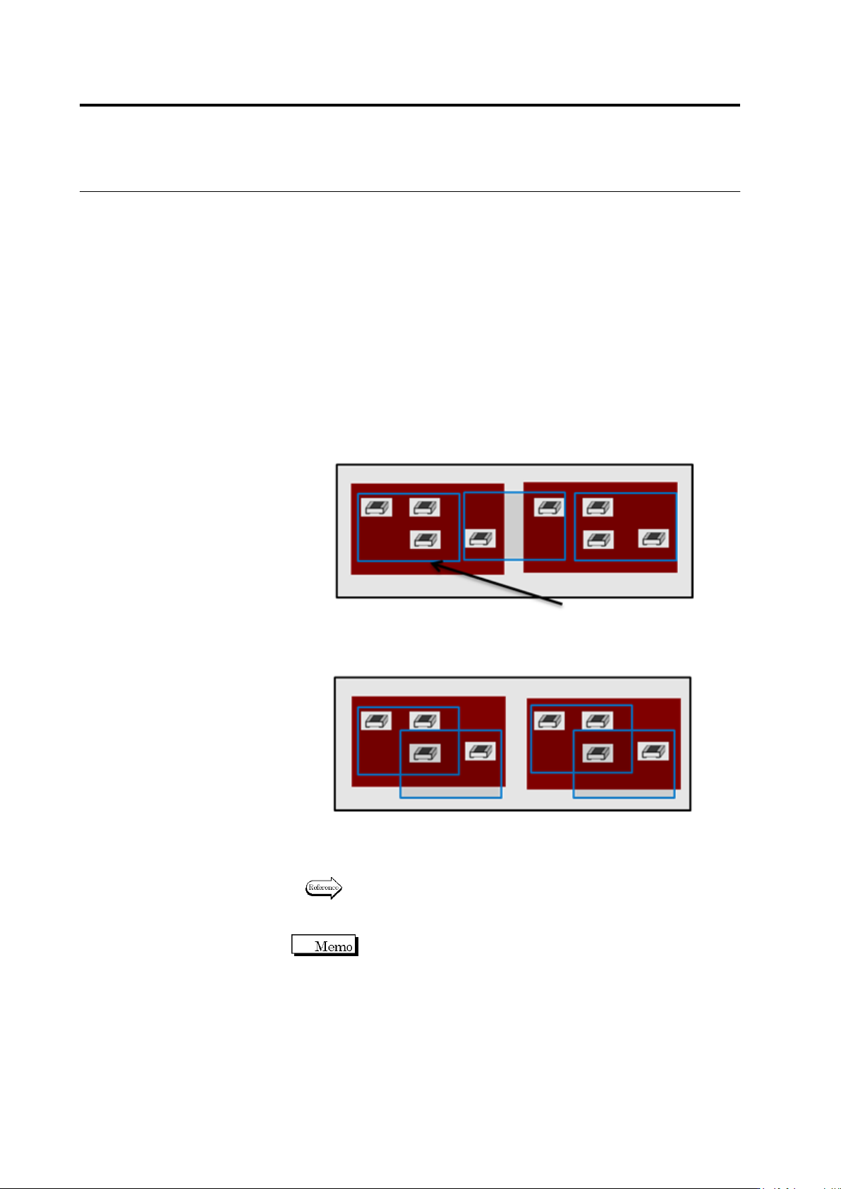
■ Adjust Block Position Individually (position correction for each
component block unit)
This is a function to determine FOV so that one FOV is not
applicable to inspection of a component which has multiple
component block units.
Use this function when inspecting a flexible PCB and so on, which
means that the status of position shift (direction and/or quantity) is
different for each component block unit.
This function can be set up on v-TS for each inspection program,
so that whether to perform position correction for each component
block unit can be set up. To set it up, click the checkbox to specify
ON/OFF.
FOV is arranged like the figures above, and positions are
corrected in each FOV.
For details of this function, refer to Section 2.3 “Inspection
Screen Position Correction” of the inspection logic manual.
When setting ON this function, be careful of the following. Do not
setting it ON unless needed.
1) Since the number of inspection FOV increases, tact time
becomes longer.
2) Since the search range of position correction is broad, the
matching rate of binarized images by pattern matching might
become low, so the risk of failing position correction increases.
<Position correction for each component block unit: OFF>
Component block unit 1 Component block unit 2
FOV (blue frame)
<Position correction for each component block unit: OFF>
Component block unit 1 Component block unit 2
2.2 Creating a New Inspection Program
2-29
書式変更: フォント : (日) MS ゴシッ
ク, 10 pt
削除: Creating a New Inspection Progra
m
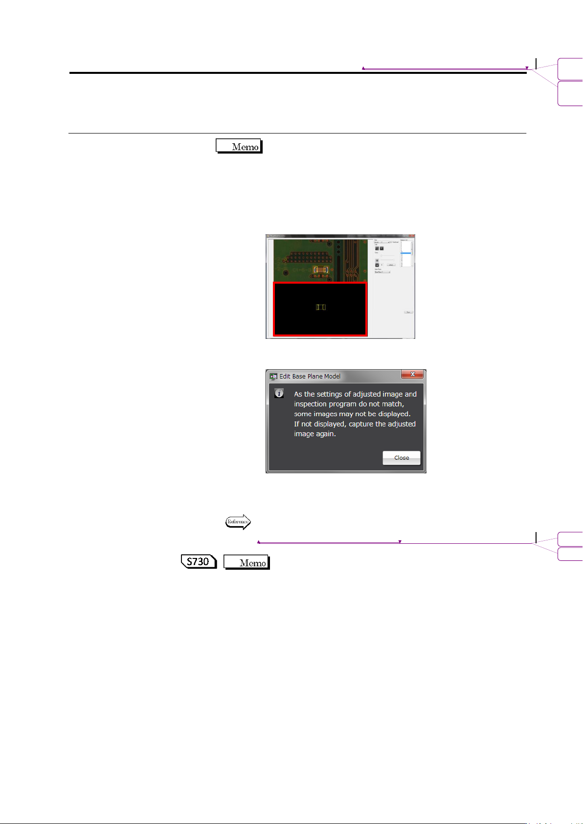
Be careful about the following after setting ON/OFF this function:
Since the FOV is changed, teaching which uses adjustment
images, such as PCB test or reference face model editing, might
not be performed correctly due to the following phenomena:
[Phenomena]
1) A false call occurs (during the PCB test)
2) A black image is displayed (when a reference level model is
edited)
(Ex.: Reference level model editing screen inside the red frame)
3) A warning dialog is displayed.
(when starting up reference level model editing)
For the countermeasures, obtain the adjustment image again
after switching ON and OFF.
For editing of a reference level model, refer to Section 2.16.4
“Editing a Reference Level Model.”
Editing of a reference face model is effective for S730 only.
書式変更: フォント : (英) Arial
削除: Editing a Reference Level Model
Chapter 2 Inspection Programming
2-30
■ Width (mm)
Enter the horizontal PCB size (Unit: mm).)
A value in the range of 50.00 to 510.00, up to two decimal
places can be entered.
The width cannot be changed once specified.
■ Height (mm)
Enter the vertical PCB size (Unit: mm).
A value in the range of 50.00 to 460.00, up to two decimal
places can be entered.
The height cannot be changed once specified.
The offset value can be changed after it is set, depending on
the PCB variations. The offset value can be specified up to the
first decimal place within the range from -0.5 to 0.5, which is
retained in individual inspection programs.
Refer to "2.18.5 Renaming an Inspection Program" for
the procedure to change the value.
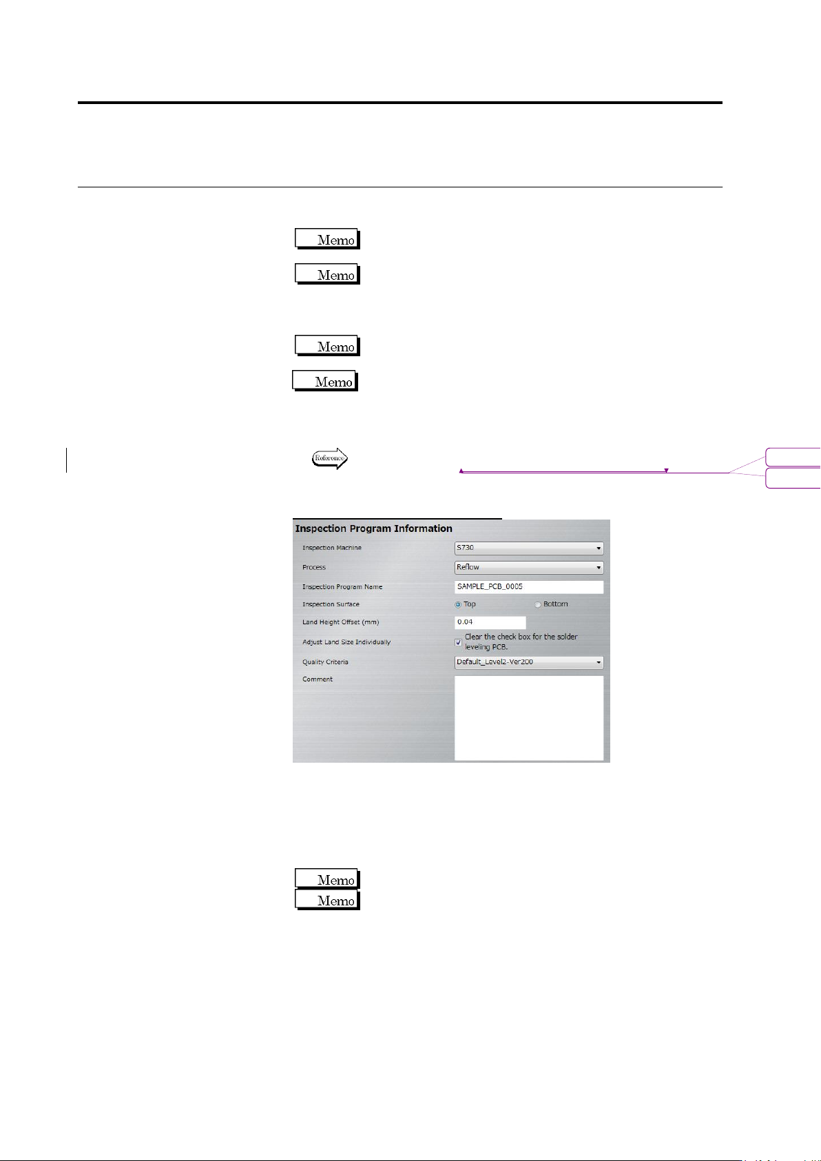
Inspection Program Information
■ Inspection Machine
Select the inspection machine to use for capturing the PCB image
in the pull-down menu.
■ Inspection Program Name
Enter the name of a new inspection program within 48 single-byte
alphanumeric characters/symbols.
Symbols that can be used: ! # $ % & ' ( ) - = ^
~
@`[ { ;+ } ] ,._␣
Both upper and lower case alphabet characters can be used.
However, they are not distinguished.
書式変更: フォント : Arial
削除: Renaming an Inspection Program