Omron V-TS Teaching Manual.pdf.pdf - 第219页
Chapter 2 Insp ection Progr amming 2- 192 3. Select the character istic param eter to edit from the options: Position Adjustment Color, So lder Color, Lan d Exposed Color, Fillet-Excluded Co lors and PCB Co lor. Edit the…
2.16 Managing PCB Images
2-191
2.16.3 Editing Models by the Unit of PCB
This section describes a procedure to edit the model on a per PCB basis.
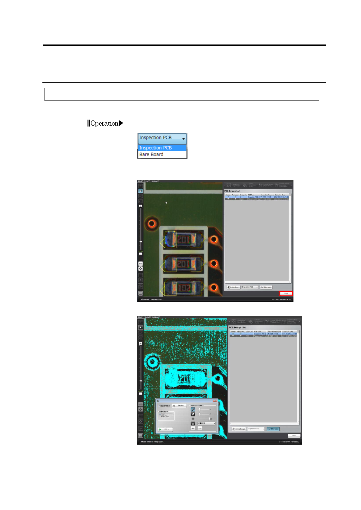
1.
Select "Inspection PCB" in the PCB Image Management screen if
the Board Image List contains bare board images.
2.
Click to select the inspection PCB image to edit in the Board Image
List and click [Edit Model].
The color table editing tool is displayed.
Operation
Chapter 2 Inspection Programming
2-192
3.
Select the characteristic parameter to edit from the options: Position
Adjustment Color, Solder Color, Land Exposed Color,
Fillet-Excluded Colors and PCB Color. Edit the color table.
Each characteristic parameter is used on the inspection items
shown below.
- Position Adjustment Color ... Inspection Screen Position
Adjustment
- Solder Color ... Component Presence, Solder Ball,
Solder Bridging
- Exposed Land Color ... Exposed Basis Metal, Missing
Component
- Fillet-Excluded Colors ... Fillet Inspection
- PCB Color ... Missing Component, Foreign Material
Refer to each inspection item in the Inspection Logic Manual for colors
to be extracted.
Refer to "Model Editing Screen Operation" for the color table editing
tool operation.
When you select the PCB Color or Position Adjustment Color, the
[Re-extract Color] button is enabled and each color is automatically
extracted and displayed.
The [Test] button is enabled only when you select the position
adjustment color. When you click it the land window after position
adjustment is displayed.
Only the land window of the component displayed on the
screen when [Test] was clicked.
4.
As the criterion for screen position correction, either [Land] or
[Wiring Pattern] can be selected.
[Land] is selected by default. If post-mounting inspection is
conducted and it is detected that solder paste extends beyond
the land, or if a lot of bottom electrode components such as
BGA are implemented and the land is not visible, select [Wiring
Pattern].
2.16 Managing PCB Images
2-193
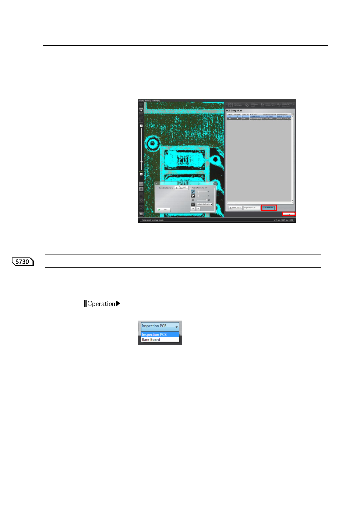
5.
Clicking [Edit Model] again closes the color table editing toolbox.
Click [Close]. The Inspection Program Editing screen returns.
2.16.4 Editing a Reference Level Model
When conducting inspection or v-TS PCB tests by the system, if a measured component height is
different from the height of the real component, use the reference level model editing tool to edit
the reference level model. This section describes the operation procedure of this tool.
1.
On the menu bar of the edit screen, select [Tool] - [PCB Image
Management Screen]. If a bare board image is displayed on the
screen, select Inspection PCB from the list.