KJ-01.02.Instruction Manual.REV.02.pdf - 第110页
5 − 14 (3) PW B config uration 1) Single PW B The PW B which has only one circuit pattern. Figure 5.3.2.4 Fi gure of the single pattern 2) Multiple PW B matrix The PW B which has multiple circuit pat terns alig ned in de…
5 − 13
For the basic setup change screen, the following items are to be entered. To change
to another item, use the TAB key or the TAB and SHIFT keys.
(1) PWB ID
Up to 32 alphanumeric characters and symbols can be entered. However, note
that only numbers or only symbols cannot be entered. They shall be combined
with alphabetic characters. When reading the production program, the PWB ID is
displayed as well as the file name of the production program, so enter an ID
which is easy to understand.
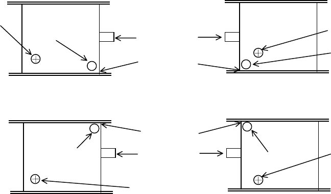
(2) Reference method
1) Hole reference
The PWB has positioning holes, and the reference pins are inserted in the
holes to hold the PWB.
2) Shape reference
After the PWB touches the stopper, the edges of the PWB are fixed
mechanically to hold the PWB.
①
①①
①
Front reference ②
②②
②
Front reference
③
③③
③
Rear reference ④
④④
④
Rear reference
Figure 5.3.2.3 Positioning hole position and the shape reference position
Board transport direction: from left to right Board transport direction: from l right to left
Origin of a board
Board
Positioning hole
Stopper pin
Shape reference
position
Origin of a board
Positioning hole
Board transport direction: from left to right Board transport direction: from l right to left
Board
Positioning hole
Board
Positioning hole
Origin of a board
Origin of a board
Stopper pin
Shape reference
position
5 − 14
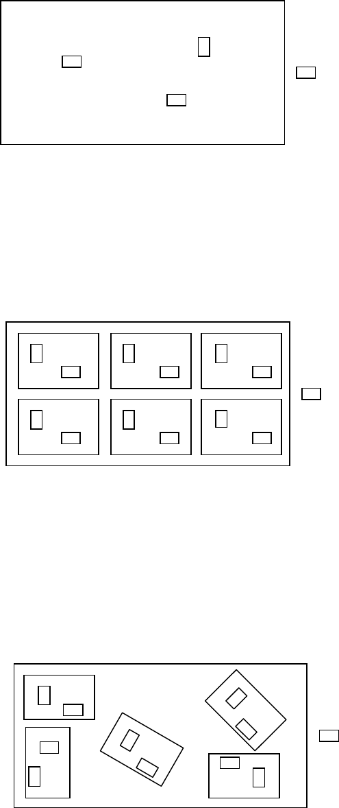
(3) PWB configuration
1) Single PWB
The PWB which has only one circuit pattern.
Figure 5.3.2.4 Figure of the single pattern
2) Multiple PWB matrix
The PWB which has multiple circuit patterns aligned in depth and width and
with a same angle and space.
Figure 5.3.2.5 Figure of the Matrix multiple patterns
3) Multiple PWB non-matrix
The PWB which has multiple circuit patterns but with a different angle and
space among them.
Figure 5.3.2.6 Figure of the Non-matrix multiple patterns
Components
Components
Components
5 − 15
(4) BOC type
1) Not used
Production is carried out not using the BOC mark. (The mark printed on the
PWB and to be used for offsetting the placement point. See 5. Board
Recognition Marks of 1.1.7 Printed circuit board specifications.)
2) PWB mark is used
A set of BOC marks are used for the placement point offset of the entire
PWB area. When the BOC mark is used for a single pattern PWB, select
this item. When a set of BOC marks is used for the entire area of a multi
pattern PWB, select also this item.
3) Circuit mark is used
For a multiple pattern PWB, when the BOC mark of each pattern is used for
the placement point offset of each circuit of the PWB, select this item.
Accuracy of placement is better compared with the placement using the
BOC
(5) Bad mark type
1) Not used
Select this item when production is carried out without using bad marks.
(The bad marks are used for recognizing a certain circuit of a multiple
pattern PWB where components are not to be mounted. Normally, sealing or
painting is applied for the bad marks.) For a single pattern PWB, the bad
marks cannot be used, and select this item.
2) Mark is light
Select this item when a bad mark and the PWB are recognized with the bad
mark sensor, and the reflection ratio of the bad mark is higher than that of
the PWB.
3) Mark is dark
Select this item when a bad mark and the PWB are recognized with the bad
mark sensor, and the reflection ratio of the bad mark is lower than that of the
PWB. This item shall be selected particularly when black bad marks are
used on a ceramic board.