KJ-01.02.Instruction Manual.REV.02.pdf - 第28页
1 − 12 Note: For t he shape of chip components t o be mounted (1) For the parts whose shape is cylindrical, there is no m inimum shade when turned, and chip recognit ion by laser align is ther efor e impossible. (2) A po…
1 − 11
1.1.6 Applicable components and packages
(1) Applicable component sizes (For laser recognition)
Component height : Min. 0.3 mm
Max. 12mm
Component size : Min. 0.6 X 0.3 mm
Max. 20 mm or 23.5 x 11 mm
Lead pitch : Min. 0.65 mm
(2) Applicable component sizes
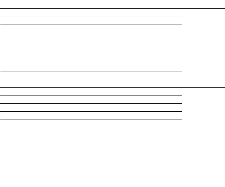
Table 1.1.6.1
Component Name and Type Package
Square chip resistor 1005, 1608, 2012, 3216, 3225 (5025, 6432), 0603
Network resistor (Excluding SOP, SOJ, PLCC types)
MELF resistor 1.6 X ø1.0, 2.0 X ø1.25, 3.5 X ø1.4, 5.9 X ø2.2 mm
Laminated ceramic capacitor 1005, 1608, 2012, 3216, 3225, 4532, 5750 (5632), 0603
Tantalum chip capacitor 3216, 3528, 6032, 7343
Aluminum electrolytic capacitor Height: 12.0 mm or less
Chip film capacitor
Variable trimmer capacitor, Chip potentiometer, trimmer
Chip ferrite beads
Chip inductor
Tape
SOT molded part 1608/2012, SOT-23, SOT-89, SOT-143, SOT-223
SOP 8, 14, 16, 18, 20, 24, 28 pin or 23.5 x 11mm or less
SOJ 16, 18, 20, 24, 26, 28 , 32pin
PLCC 18, 20, 22, 28 (Square), 28 (Rectangle), 32, 44 pins
QFP, BQFP Pitch 0.65/0.8/1.0mm 20 mm x 20 mm or less, 23.5 x 11mm or less
BGA 20 mm x 20 mm or less, 23.5 x 11mm or less
Connector
Pitch: 0.65 or more
Dimensions: 20 mm x 20 mm or less, or 23.5 mm x 11 mm or less
Recognizable with laser
IC socket
Pitch: 0.65 or more
Dimensions: 20 mm x 20 mm or less, or 23.5 mm x 11 mm or less
Recognizable with laser
Tape
Stick
Tray
1 − 12
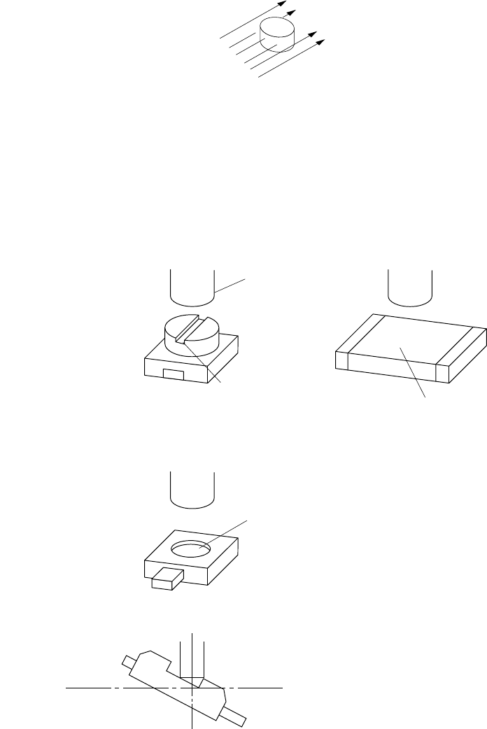
Note: For the shape of chip components to be mounted
(1) For the parts whose shape is cylindrical, there is no minimum shade when turned,
and chip recognition by laser align is therefore impossible.
(2) A poor pickup or placement accuracy could result if the top surface of the
component to be placed is curved, protruded, or dented. Avoid using such
components. (Some such components may, however, be handled by changing
the nozzle number.)
<Typical pickup failures>
MO
MO
<Typical poor placement accuracy>
Picku
p
nozzle
Slotted
g
roove
Embossed characters
Dented
Laser reco
g
nition
1 − 13
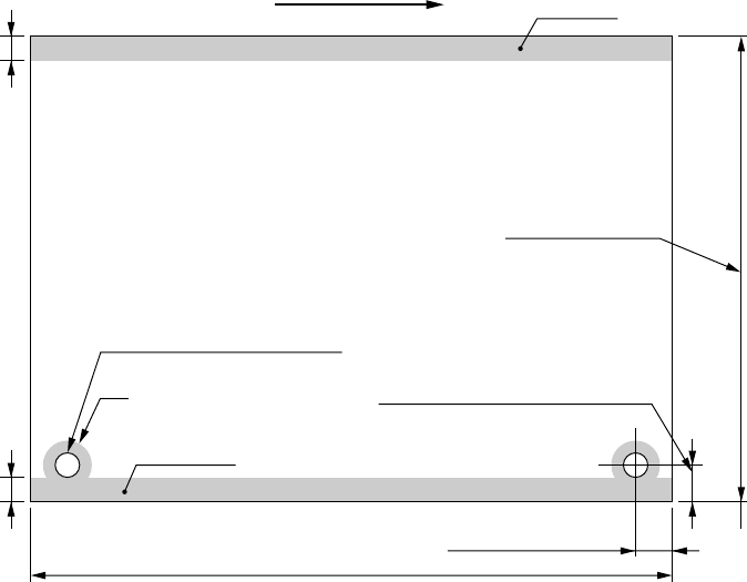
1.1.7 Printed circuit board specifications
1. Board size
Min. : X 50 mm x Y 30 mm
Max. : X 203.2 mm x Y 152.4 mm
X : Along the movement of the board
Y : From front to rear (and reversely) of the machine
2. Board thickness
Min. : 0.4 mm
Max. : 2 mm
3. Board warp limit
Free state: Upward max. 2 mm
Downward max. 5 mm
(With max. board size; for others, the value is proportional to the
diagonal length.)
At centering: Upward/downward max. 2 mm
4. Board limitations
3
3
Movement of PWB
Marginal area
30 ~ 152.4mm
φ
4
+0.1
mm
0
φ 6
Marginal area
Standard 5 ± 0.1mm
50 ~ 203.2mm
5 ± 0.1mm
Conveying rail