KJ-01.02.Instruction Manual.REV.02.pdf - 第114页
5 − 18 (3) Non-matri x multi ple pa tterns 1) Hole Ref erence Set t he distance f rom t he home position of a board to t he board positioning point (ref erence pin posit ion for “Hole ref erence,” or shape clamp ref er e…
5 − 17
(2) Matrix multiple patterns
1) Hole Reference
Set the distance from the home position of a board to the board positioning
point (reference pin position for “Hole reference,” or shape clamp reference
position for “Shape reference”).
2) First circuit
Set the coordinates of the home position of the reference circuit viewed from
the home position of a PWB.
3) Circuit division number
Set the number of circuits located in each direction with supposition that the
PWB transport direction is X, and the vertical direction is Y.
4) Circuit pitch
Set the space between the origins of the circuit patterns on the PWB by
defining X as the same direction of the PWB transport, and Y as the right
angle to the direction of the PWB transport.
5) BOC mark position
Specify the coordinates of the center point of a BOC mark. Be sure to
specify coordinates of at least two BOC marks here.
If you use a PWB mark, enter coordinates viewed from the home position of
a PWB. If you use a circuit mark, enter coordinates viewed from the home
position f a circuit.
6) Vision data
The parentheses ( ) at the right edge of the BOC mark position shows the
completeness of the vision data. When the vision data is complete, an
asterisk * appears in the parentheses ( ). For teaching of the vision data, see
6.3 “Teaching Recognition”.
7) Bad mark position
Set the distance between the origin of the circuit and the center of the bad
mark.
8) PWB height
Set the height of the top side of a board. Normally the height of the top
side of a fixed board is regarded as “0.”
Note that you have to specify the height of the side on which components
are placed if the board is placed on a jig board or like.
*1 You can use the HOD to teach the home position of a PWB, First circuit
position, BOC mark position, Bad mark position, and PWB height. See
Section 6.2 “Teaching Coordinates” for details.
*2 Total of 400 circuits can be set here.
5 − 18
(3) Non-matrix multiple patterns
1) Hole Reference
Set the distance from the home position of a board to the board positioning
point (reference pin position for “Hole reference,” or shape clamp reference
position for “Shape reference”).
2) BOC mark position
Specify the coordinates of the center point of a BOC mark. Be sure to
specify coordinates of at least two BOC marks here.
If you use a PWB mark, enter coordinates viewed from the home position of
a PWB. If you use a circuit mark, enter coordinates viewed from the home
position f a circuit.
3) Vision data
The parentheses ( ) at the right edge of the BOC mark position shows the
completeness of the vision data. When the vision data is complete, an
asterisk * appears in the parentheses ( ). For teaching of the vision data, see
6.3 “Teaching Recognition”.
4) Bad mark position
Set the distance between the origin of the circuit and the center of the bad
mark.
5) PWB height
Set the height of the top side of a board. Normally the height of the top
side of a fixed board is regarded as “0.”
Note that you have to specify the height of the side on which components
are placed if the board is placed on a jig board or like.
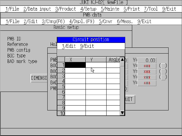
6) Circuit position
When you click the <CIRCUIT> button, the “Circuit position” window appears
on the screen (see Figure 5.3.2.7).
Use the up, down, left and/or right arrow key to enter the position. Specify
the distance from the home position of a PWB to that of each circuit as the
home position (X, Y) of a circuit. Set the angle of each circuit to the “Angle”
column.
Figure 5.3.2.7 Pattern layout
5 − 19
a) Commands available on the “Circuit position” window.
By selecting “1/ Edit”, the edit window appears.
When selecting “1/ Blank line input”, a blank line is created in the line just
above the current cursor position.
When selecting “2/ Delete”, the data on the line of the current cursor position
is deleted and the data that follows appears there.
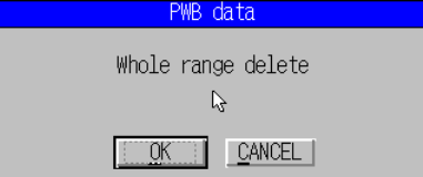
When selecting “3/ Delete all”, a dialog box which asks whether to delete all
data appears (see Figure .5.3.2.8). When the OK button is selected, all the
data of circuit position is deleted and the cursor moves to the first line.
Figure 5.3.2.8 Delete all dialog box
* 1 You can use the HOD to enter the home position of a PWB, BOC mark
position, Bad mark position, PWB height and the home position (X, Y)
of a circuit on the “Circuit position” window. See Section 6.2 “Teaching
Coordinates” for details.
* 2 Total of 100 circuits can be specified here.
* 3 When you change the PWB configuration from “Matrix PWB matrix” to
“Matrix PWB non-matrix”, the circuit settings are changed so that the
circuit angle is set to “0.”