KJ-01.02.Instruction Manual.REV.02.pdf - 第29页
1 − 13 1.1.7 Printed circuit board specifications 1. Board size Min. : X 50 mm x Y 30 mm Max . : X 203.2 mm x Y 152.4 mm X : Along the movement of the boar d Y : From fr ont to r ear (and reversely) of the m achine 2. Bo…
1 − 12
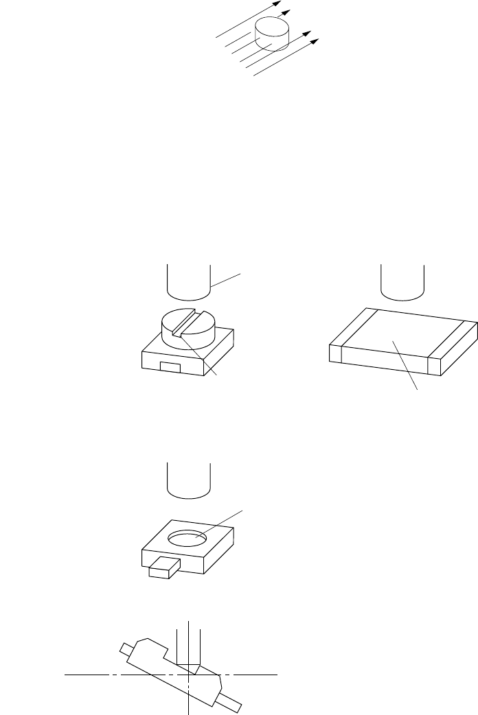
Note: For the shape of chip components to be mounted
(1) For the parts whose shape is cylindrical, there is no minimum shade when turned,
and chip recognition by laser align is therefore impossible.
(2) A poor pickup or placement accuracy could result if the top surface of the
component to be placed is curved, protruded, or dented. Avoid using such
components. (Some such components may, however, be handled by changing
the nozzle number.)
<Typical pickup failures>
MO
MO
<Typical poor placement accuracy>
Picku
p
nozzle
Slotted
g
roove
Embossed characters
Dented
Laser reco
g
nition
1 − 13
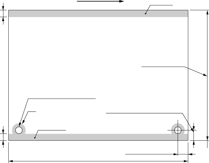
1.1.7 Printed circuit board specifications
1. Board size
Min. : X 50 mm x Y 30 mm
Max. : X 203.2 mm x Y 152.4 mm
X : Along the movement of the board
Y : From front to rear (and reversely) of the machine
2. Board thickness
Min. : 0.4 mm
Max. : 2 mm
3. Board warp limit
Free state: Upward max. 2 mm
Downward max. 5 mm
(With max. board size; for others, the value is proportional to the
diagonal length.)
At centering: Upward/downward max. 2 mm
4. Board limitations
3
3
Movement of PWB
Marginal area
30 ~ 152.4mm
φ
4
+0.1
mm
0
φ 6
Marginal area
Standard 5 ± 0.1mm
50 ~ 203.2mm
5 ± 0.1mm
Conveying rail
1 − 14
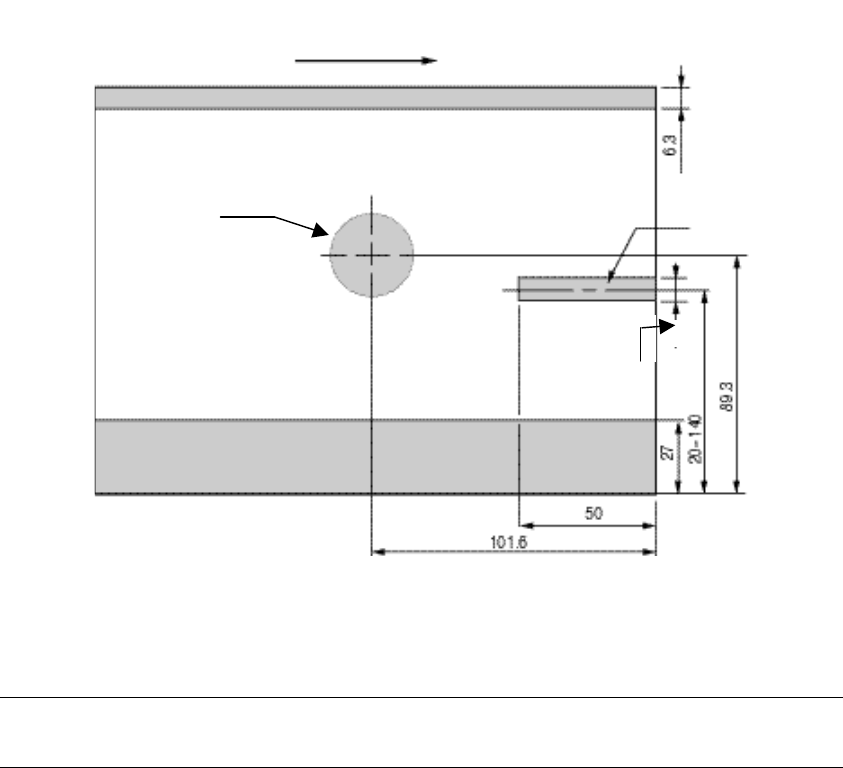
Area in which backup pins cannot be proved
φ35
22
Note: When the PWB is transferred from right to left, the marginal area of 50mm x
22mm is set on the left.
Stopper position
(Note)
(Variable)
Conveying rail (fixed)
Movement of PWB