KJ-01.02.Instruction Manual.REV.02.pdf - 第31页
1 − 15 Figure 1.1.7. 1 5. Board Recog nition Marks Create the boar d recognit ion mark s under the f ollowing conditions. (See Figure 1. 1.7.2. ) W e recommend t he f illed circle f or the m ark. The clearance ar ea arou…
1 − 14
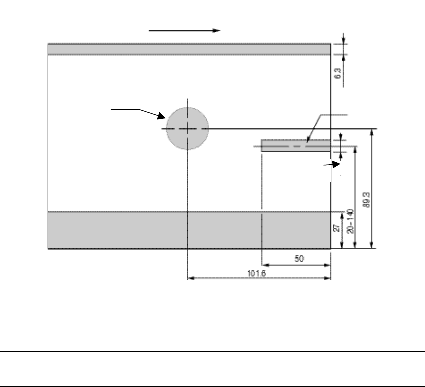
Area in which backup pins cannot be proved
φ35
22
Note: When the PWB is transferred from right to left, the marginal area of 50mm x
22mm is set on the left.
Stopper position
(Note)
(Variable)
Conveying rail (fixed)
Movement of PWB
1 − 15
Figure 1.1.7.1
5. Board Recognition Marks
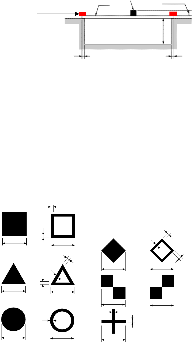
Create the board recognition marks under the following conditions.
(See Figure 1.1.7.2.) We recommend the filled circle for the mark.
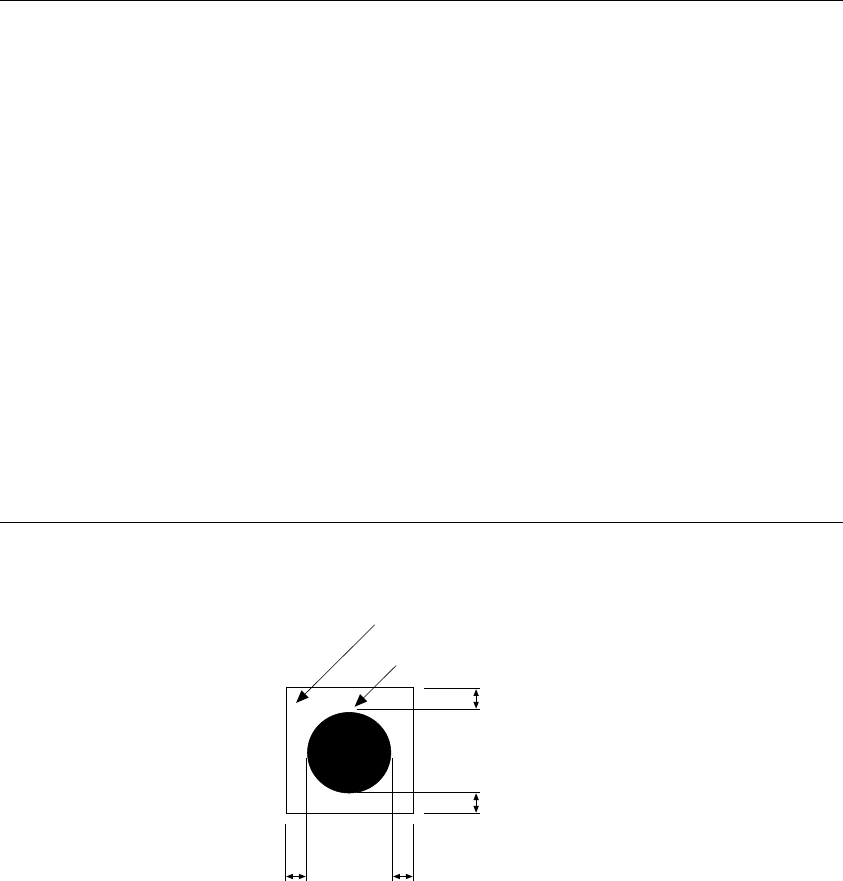
The clearance area around the mark shall be as shown in Figure 1.1.7.3.
Within this area, there shall not be any silk patterns, strip lines (including inner
layer patterns), through holes, resists, and other components.
A size: 0.5 to 3.0 mm ± 10%
B size: 0.2 mm or more
C size: 0.5 to 3.0 mm ± 10%
A
B
B
B
A
A
A
C
B
C
C
C
C
A
B
A
B
B
B
B
B
B
Figure 1.1.7.2
Component
PWB
12 mm
MAX 20 mm
3
3
Guide rail
Marginal area
on the back
of PWB
1 − 16
Notes: 1. When recognition, the mark shall be placed in the angle shown above.
However, if you specify "Use of each circuit mark" for a non-matrix
PWB, the mark can be recognized only when all marks of the
reference circuit are positioned in the angle described and the circuit is
positioned at 90, 180, 270 or 360 degrees.
2. The fiducials of the same shape and same size is preferable within a
board.
3. When processing, copper foil or solder plating can be recognized.
4. Maximum number of marks which can be registered
Board mark: 1 set (2 marks or 3 marks)
IC mark: 50 sets (Pairs of 2 marks)
5. Items that can be registered
Mark number
Balance detection window
Normal/reverse rotation identification when detected
Mark shape
Outer dimensions
Figure 1.1.7.3
Clearance area
Recognition mark
0.5 mm or more
0.5 mm or more
0.5 mm or more