KJ-01.02.Instruction Manual.REV.02.pdf - 第30页
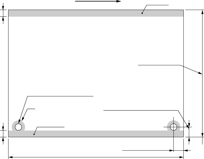
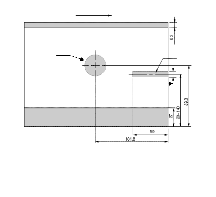
1 − 14 Area in which backup pins cannot be proved φ 35 22 Note: When the PWB is transferred from right to le ft, the marginal area of 50mm x 22mm is set on the l eft. Stopper position (Note) (V ariable) Conveying rail (f…
1 − 13
1.1.7 Printed circuit board specifications
1. Board size
Min. : X 50 mm x Y 30 mm
Max. : X 203.2 mm x Y 152.4 mm
X : Along the movement of the board
Y : From front to rear (and reversely) of the machine
2. Board thickness
Min. : 0.4 mm
Max. : 2 mm
3. Board warp limit
Free state: Upward max. 2 mm
Downward max. 5 mm
(With max. board size; for others, the value is proportional to the
diagonal length.)
At centering: Upward/downward max. 2 mm
4. Board limitations
3
3
Movement of PWB
Marginal area
30 ~ 152.4mm
φ
4
+0.1
mm
0
φ 6
Marginal area
Standard 5 ± 0.1mm
50 ~ 203.2mm
5 ± 0.1mm
Conveying rail
1 − 14
Area in which backup pins cannot be proved
φ35
22
Note: When the PWB is transferred from right to left, the marginal area of 50mm x
22mm is set on the left.
Stopper position
(Note)
(Variable)
Conveying rail (fixed)
Movement of PWB
1 − 15
Figure 1.1.7.1
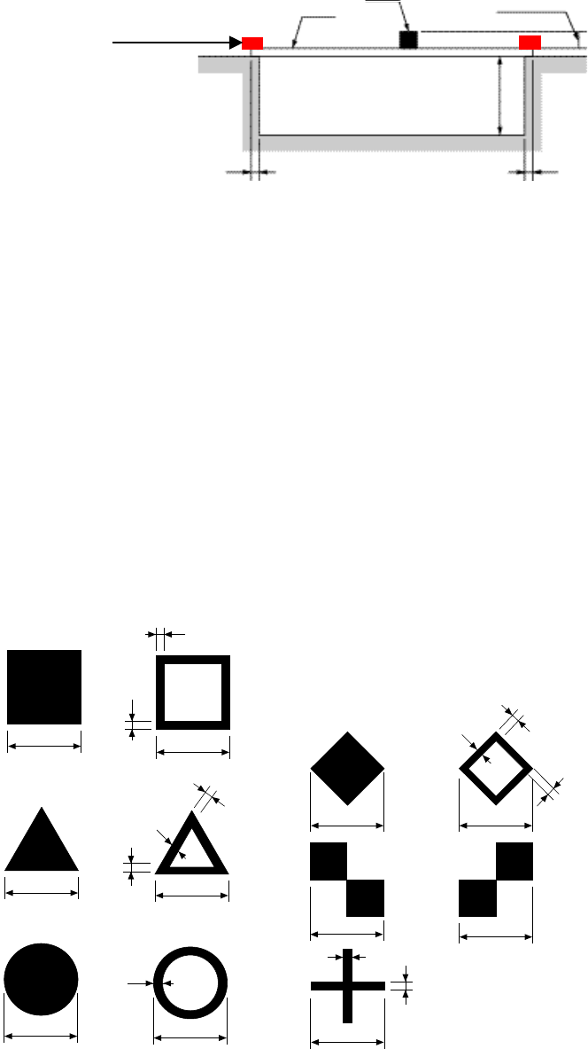
5. Board Recognition Marks
Create the board recognition marks under the following conditions.
(See Figure 1.1.7.2.) We recommend the filled circle for the mark.
The clearance area around the mark shall be as shown in Figure 1.1.7.3.
Within this area, there shall not be any silk patterns, strip lines (including inner
layer patterns), through holes, resists, and other components.
A size: 0.5 to 3.0 mm ± 10%
B size: 0.2 mm or more
C size: 0.5 to 3.0 mm ± 10%
A
B
B
B
A
A
A
C
B
C
C
C
C
A
B
A
B
B
B
B
B
B
Figure 1.1.7.2
Component
PWB
12 mm
MAX 20 mm
3
3
Guide rail
Marginal area
on the back
of PWB