IPC-TM-650 EN 2022 试验方法.pdf - 第103页
T able 1 T est Report on Solder Paste Enter appropriate information in top portion of report and complete report by entering the test results or checkmarks in the appropriate spaces. Inspection Purpose: QPL I.D. Number: …

1.0
Scope
This
procedure determines the percent metal
content for solder paste.
2.0
Applicable Documents
None
3.0
Test Specimen
50
grams of solder paste
4.0
Equipment/Apparatus
Balance
Crucible
or Beaker
Heat Source
Flux Solvent
5.0
Procedure
5.1 Preparation
5.1.1
Weigh
10 to 50 grams (to the nearest 0.01 gram) of
solder paste into a tared vessel suitable for melting the solder
paste.
5.2
Test
5.2.1
Melt
the solder at approximately 25°C above liquidus
of the alloy, remove from heat and allow solder to solidify.
5.2.2
Extract
melt from residual flux with a suitable solvent,
dry and weigh metal to within 0.01 grams to determine %
metal content.
5.3
Evaluation
Weight
of extracted metal
Weight
of original sample
x 100 = % Metal
Enter the results in Table 1 ‘‘Test Report on Solder Paste.’’
The
Institute for Interconnecting and Packaging Electronic Circuits
2215 Sanders Road • Northbrook, IL 60062
IPC-TM-650
TEST
METHODS MANUAL
Number
2.2.20
Subject
Solder
Paste Metal Content by Weight
Date
1/95
Revision
Originating Task Group
Solder Paste Task Group (5-24b)
Material
in this Test Methods Manual was voluntarily established by Technical Committees of the IPC. This material is advisory only
and its use or adaptation is entirely voluntary. IPC disclaims all liability of any kind as to the use, application, or adaptation of this
material. Users are also wholly responsible for protecting themselves against all claims or liabilities for patent infringement.
Equipment referenced is for the convenience of the user and does not imply endorsement by the IPC.
P
age1of2
电子技术应用 www.ChinaAET.com
T
able 1 Test Report on Solder Paste
Enter appropriate information in top portion of report and complete report by entering the test results or checkmarks in the appropriate spaces.
Inspection Purpose: QPL I.D. Number:
__
Qualification Manufacturer’s Identification:
__ Quality Conformance A Manufacturer’s Batch Number:
__
Quality Conformance B Date of Manufacture:
__
Shelf-Life Extension Original Use-By Date:
__
Performance Revised Use-By Date:
Date
Inspection Completed:
Overall
Results: __ Pass __ Fail
Inspection Performed by:
W
itnessed by:
Inspections
User’s
Actual
Requirement Test Result P/F (*) Tested by & Date
Material
Visual
Metal Content
Viscosity
Solder Ball
Slump
Alloy
Flux
Powder Size
% In Top Screen
% In Next Screen
% In Bottom Screen
% In Receiver Bottom
Max. Powder Size
Powder Shape
Tack
Wetting
* P/F = PASS/FAIL; enter P if test results are within tolerance of actual requirement; otherwise, enter F
IPC-TM-650
Number
2.2.20
Subject
Solder
Paste Metal Content by Weight
Date
1/95
Revision
P
age2of2
电子技术应用 www.ChinaAET.com
1
Scope
The
object of a planarity measurement is to deter-
mine the effectiveness of a polymer thin film in smoothing
topological features created by underlying layers of circuitry or
etch patterns. In this case, the polymer thin film is a dielectric
material for use in High Density Interconnect (HDI) and
microvia technologies.
1.1
Test Structure
Schematics
given in Figure 1 (end view)
and Figure 2 (top view) depict the essential features of a rec-
ommended test structure for measuring the planarity as a
function of feature size.
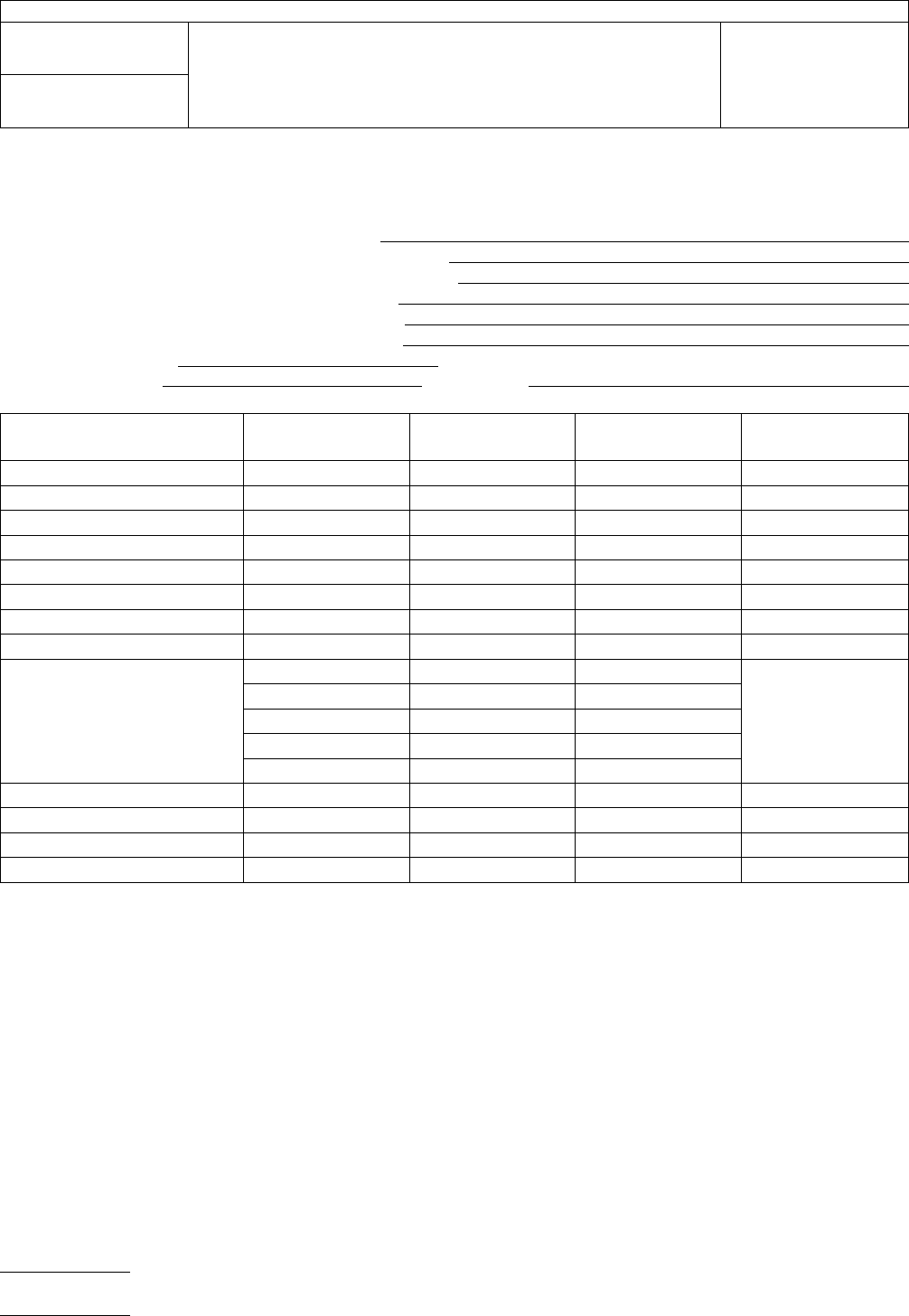
In the finished test structure, ‘‘d’’ is the step height over the
circuit trace after the polymer has been deposited and cured.
The planarity is dependent on the trace height, ‘‘b,’’ the poly-
mer coating thickness, ‘‘c,’’ and the trace width, ‘‘a.’’ Rather
than fully characterizing this relationship for each polymer
coating, it is best to use simplified standard procedures for
measurement and for comparing different types of coatings.
Planarity is also affected by the proximity of the line feature
being used for measurement to any neighboring topological
feature in the test structure. Planarity is generally much lower
for isolated features. Therefore, in order to consider the
‘‘worst case’’ conditions, isolated lines are preferred in the
test structure. To satisfy this requirement, no neighboring fea-
tures can be within fewer than 15 line widths of the line in
question.
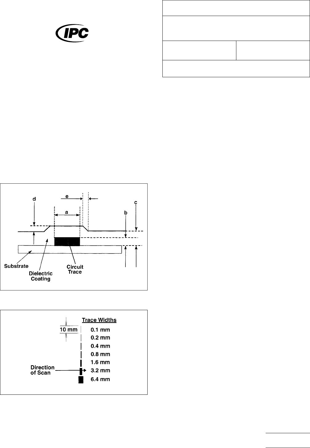
The test pattern in Figure 2 is recommended as one that pro-
vides planarity characterization over a broad range of feature
sizes. All lines are isolated in accord with the above guideline.
It is recommended planarity be determined over the complete
range of these widths (but the specific nominal values within
that range are not important). Normally, one finds the planar-
ity is high over narrow lines, but it progressively rolls off in pro-
ceeding toward wider ones. The roll-off rate is important, and
it varies from polymer to polymer. Thus any report of planarity
must include the line width measured and, preferably, a plot of
planarity versus line width should be reported.
2
Applicable Documents
IPC-DD-135
Qualification
for Deposited Organic Interlayer
Dielectric Materials for Multi-Chip Modules
3
Test Specimens
3.1 Prepare Test Coupons
Prepare
the surface of the test
structure for polymer deposition in accordance with the pro-
cedure recommended by the manufacturer of the dielectric
coating (follow all procedures for cleaning the surface and for
deposition of a coupling agent if one is recommended). Coat
the polymer resin in accordance with the manufacturer’s rec-
ommended procedure to provide an average film thickness of
63.5 µm (± 10%) for 18 µm copper over the substrate surface
when the cure is completed. Cure the polymer thin film using
IPC-2-2-21-1
Figure 1 Cross-Section Planarization Diagram
IPC-2-2-21-2
Figure
2 Top View of Planarization Structure
The
Institute for Interconnecting and Packaging Electronic Circuits
2215 Sanders Road • Northbrook, IL 60062
IPC-TM-650
TEST
METHODS MANUAL
Number
2.2.21
Subject
Planarity
of Dielectrics for High Density
Interconnection (HDI)/Microvia Technology
Date
11/98
Revision
Originating Task Group
HDI Test Methods Task Group (D-42a)
Material
in this Test Methods Manual was voluntarily established by Technical Committees of the IPC. This material is advisory only
and its use or adaptation is entirely voluntary. IPC disclaims all liability of any kind as to the use, application, or adaptation of this
material. Users are also wholly responsible for protecting themselves against all claims or liabilities for patent infringement.
Equipment referenced is for the convenience of the user and does not imply endorsement by the IPC.
P
age1of4
电子技术应用 www.ChinaAET.com