IPC-TM-650 EN 2022 试验方法.pdf - 第645页
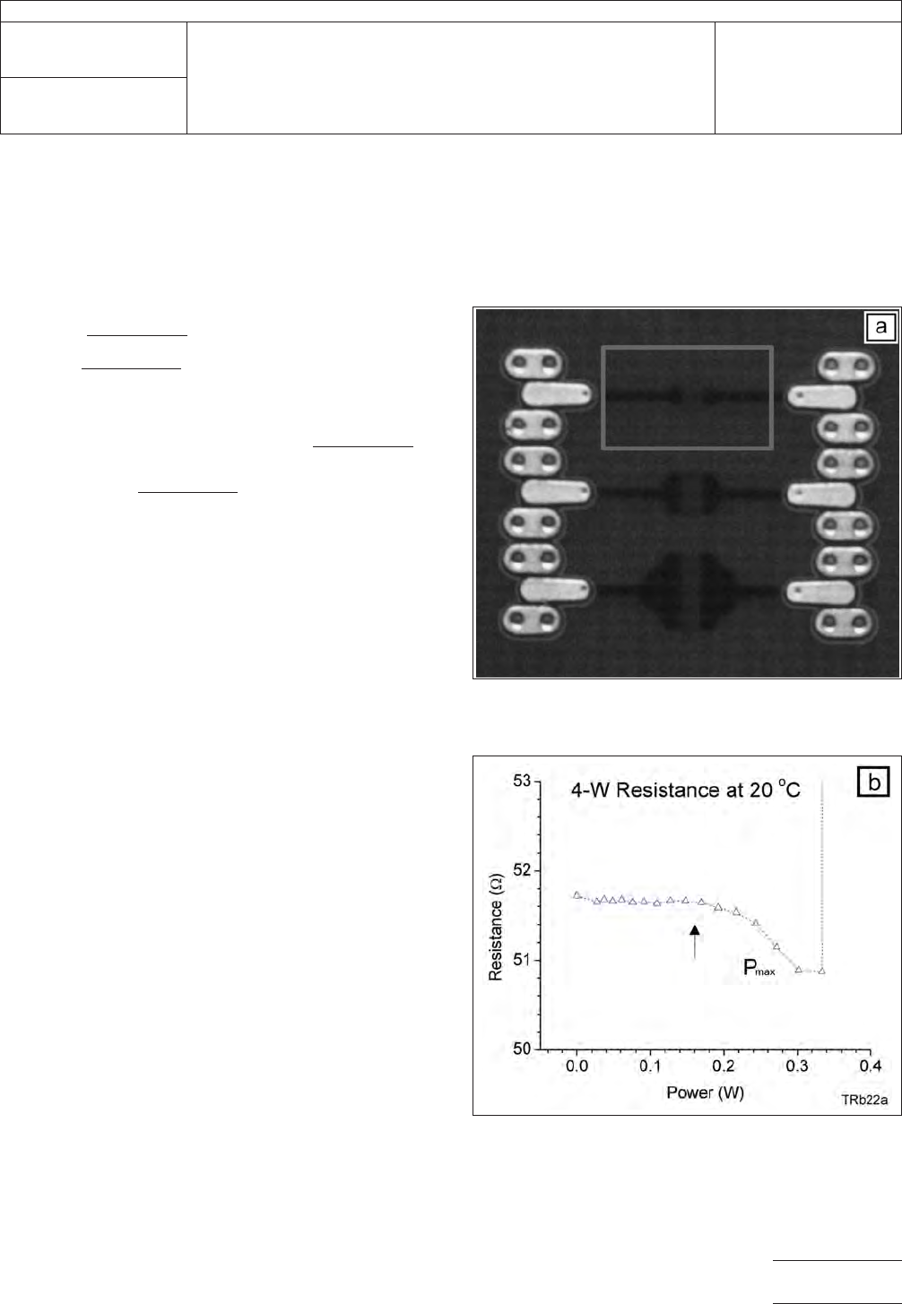
level approaches 0.160 W. With increasing power above 0.160 W the resistance value gradually starts to deviate from its stable value. The resistor fails ‘‘open’’ at P failure of 0.360 W. The resistance plot in Figure 2b …
Example: R
n
= R
0
=50Ω, I
0
=14mA,I
s
= 6 mA. At n =11
step I
11
= 80 mA and the corresponding applied power P
11
=
(0.014A+11
*
0.006 A)
2
*
50 Ω = 0.32 W.
5.3.3 Linear Power Steps Setting the voltage or current
stimulus for linear increase in the applied power is given by (7)
and (8) respectively:
V
n
=
√
(P
0
+ nP
s
)
*
R
n
(7)
I
n
=
√
(P
0
+ nP
s
) / R
n
(8)
Example: R
n
= R
0
=50Ω, P
0
= 0.01 W, P
s
= 0.01 W. At step
n = 11 the applied power P
11
=0.01+11
*
0.01 = 0.12 W.
The corresponding voltage stimulus V
11
=
√
0.12 W
*
50 Ω≈
2.5 V. In the case of sourcing current the corresponding cur-
rent stimulus I
11
=
√
0.12 W / 50 Ω≈0.048 A.
6 Procedure Testing should be performed at ambient con-
ditions; temperature (t
0
)=22°C±3°C[71.6 °F ± 5.4 °F] and
relative humidity (RH
0
) = 50% ± 10% (see IPC-TM-650,
Method 1.3, Ambient Conditions).
6.1 Measure the initial stable resistance, R
0
at the ambient
temperature (t
0
) and relative humidity (RH
0
).
6.2 Apply a constant power step P
n
for a period of 60 s,
until temperature stabilizes and a steady current reading is
reached (see 5.3).
6.3 Record voltage V
n
and the resulting current I
n
. Calculate
the actual P
n
from equation (2).
6.4 Disconnect the power for a period of time sufficient for
the device to return to the ambient temperature conditions t
0
.
Measure the device resistance R
n
. Calculate the relative differ-
ence between the measured resistance and the nominal resis-
tance:
(ΔR)
r
=(R
n
− R
0
) / R
0
(9)
6.5 Continue stepping up the applied power (6.2 - 6.4) for
P
max
and/or P
failure
until the relative change in resistance, (ΔR)
r
=(R
n
- R
0
)/R
0
approaches a value indicative of failure or
acceptance criteria.
6.6 After recording P
max
, calculate PDR using equation (4).
7 Test Example An embedded resistor R
0
=50Ω, S =
0.77 mm
*
0.58 mm ≈ 0.44 mm
2
, shown in Figure 2a was
tested under the following conditions:
Power Stimulus: Linear voltage steps (5.3.1), P
0
= 0.01 W, V
0
= 0.7 V, V
s
= 0.2 V, power step ON = 60 s.
Recording: current I
n
, voltage V
n
, power P
n
.
Power OFF Step: 20 s (typical). Recording 4-W resistance R
n
.
Figure 2b illustrates the test results. The stable resistance
value R
0
is about 51.7 Ω. It remains stable until the power
Figure 2 (a) Embedded resistor test vehicle. The device
tested on a probe station is highlighted.
Figure 2 (b) Recorded resistance R
n
as a function of
applied power P
n
.
IPC-TM-650
Number
2.5.34
Subject
Power Density Rating for Embedded Resistors
Date
07/12
Revision
Page3of4

level approaches 0.160 W. With increasing power above
0.160 W the resistance value gradually starts to deviate from
its stable value. The resistor fails ‘‘open’’ at P
failure
of 0.360 W.
The resistance plot in Figure 2b suggests that P
max
≈0.160 W.
Thus in the above illustration, the power density rating for that
resistor, for which S ≈ 0.44 mm
2
, calculated from equation (4),
PDR = 0.16 W / 0.44 mm
2
≈ 0.36 W / mm
2
.
7.1 PDR Safety Factor In the example above, the surface
temperature at the tested resistors measured (optionally) at P
n
= 0.160 W was about 42 °C. Depending on the material’s
physical characteristics, this heating effect might lead to an
accelerating aging and shortening the device operational life.
Therefore it is recommended that P
max
is reduced accordingly
by a certain safety factor that can be deduced, for example,
from the aging study.
8 Accuracy Considerations Several uncertainty factors
such as instrumentation, dimensional uncertainty of the test
specimen geometry, resistance of contacts and interconnects
among others contribute to the combined uncertainty of the
measurements. The complexity of modeling these factors may
be considerably higher when the measurements are per-
formed at elevated temperatures for resistors embedded in
complex multilayer assemblies. Adequate analysis can be per-
formed, however, using the partial derivative technique for
equation (4) It is recommended that the combined instrumen-
tation uncertainties should be 10 times smaller than the nomi-
nal tolerance value of the resistor. Likewise, it is recom-
mended that uncertainty in the surface area, S, is considered
very carefully since S is the primary parameter used in scaling
the PDR ratings for different form-factor resistors.
Additional limitations may arise from the systematic uncer-
tainty of the particular instrumentation, calibration standards,
and the dimensional imperfections of the actually imple-
mented test specimen. The test may require specialized
instrumentation when P
n
approaches the instrument maxi-
mum power compliance conditions before P
failure
is reached.
9 Notes
9.1 Resistor De-Rating
In engineering practice and in typi-
cal manufacturer specifications, resistor power ratings is nor-
mally specified at +25 °C. The power rating is reduced as the
resistor operational temperature increases. A de-rating chart
is often employed, with de-rating typically starting at 70 °C.
Power de-rating charts are often included in manufacturers’
specifications to be considered as a general guideline when
projecting the power rating for application specific conditions.
The safest design rules recommend using the largest geo-
metrical size and assuming conservative (higher than actual)
operating temperatures.
In the case of embedded resistive devices operating at tem-
perature conditions above 25 °C, the heat dissipation is highly
nonlinear with additional complexity resulting from a particular
package design. In the presented example the tested resistor
failed ‘‘open’’ at the temperature t
failure
≈ 52 °C, while the
stable P
max
corresponded to temperature t
max
≈ 38 °C. The
operational temperature of embedded resistors may vary con-
siderably, depending on construction, materials and manufac-
turing technology of the embedded package. Consequently, a
reliable universal de-rating chart cannot be constructed, and
therefore, it is recommended that the power rating be deter-
mined at the specific operating conditions of the device
according to procedure described in this document, rather
than estimated from a power de-rating chart.
9.2 Hazards During testing, a high voltage and current may
be present. The experimental set-up must be properly insu-
lated with wiring properly grounded to minimize the possibility
of electrical shock. This test may cause burning of the resis-
tive material, which in turn may produce hazardous sub-
stances resulting from material decomposition and possible
subsequent chemical reactions. In all cases, the exposure lim-
its and guidance that are set by government agencies should
be observed.
The Notes section is to be used to discuss any special con-
siderations, or detail other reference documents necessary or
recommended for the test. This section should include any
safety precautions, hazard information, or warning statements
necessary for the safe completion of the test method. This
section should also be used to show sources of obtaining
specialized test apparatus or materials for the test.
10 References and Contact Information
Jan Obrzut, National Institute of Standards and Technology
(NIST), jan.obrzut@nist.gov;
Jason Ferguson, Naval Surface Warfare Center (NSWC
Crane), jason.ferguson@navi.mil;
Michael Azarian, Center for Advanced Life Cycle Engineering
(CALCE), University of Maryland, mazarian@umd.edu.
IPC-TM-650
Number
2.5.34
Subject
Power Density Rating for Embedded Resistors
Date
07/12
Revision
Page4of4

1 Scope The fungus resistance test is used to determine
the resistance of materials to fungi and to determine if such
material is adversely affected by fungi under conditions favor-
able for their development, namely high humidity, warm atmo-
sphere, and presence of inorganic salts.
2 Applicable Documents None
3 Test Specimen Specimens must be a minimum size of
50 mm x 50 mm [1.97 in x 1.97 in] with copper foil (if appli-
cable) removed by etching using standard commercial prac-
tices.
4 Apparatus and Reagents
4.1 Test Chamber
The incubator shall be capable of main-
taining 30±1°C[86±2°F]and95±2%relative humidity
and have an ultraviolet (360 nm) source for subsequent
decontamination. Provisions shall be made to prevent con-
densation from dripping on the test item. There shall be free
circulation of air around the test item and the contact area of
fixtures supporting the test item shall be kept to a minimum.
4.2 Sterilizer
4.3 Centrifuge
4.4 pH Meter
4.5 Colony Counter
4.6 Incubator
4.7 Dishwasher
4.8 Petri Dishes
4.9 Filter Paper
4.10 Media Solutions
4.11 Microorganisms
4.12 Atomizer, 15,000 ± 3000 spores
5 Procedures
5.1 Preparation of Test Media
5.1.1 Mineral-Salts Solution
Prepare the solution to contain the following:
Potassium dihydrogen orthophosphate (KH
2
PO
4
) .......... 0.7g
Potassium monohydrogen orthophosphate (K
2
HPO
4
) ... 0.7g
Magnesium sulfate heptahydrate (MgSO
4
c7H
2
O) ........... 0.7g
Ammonium Nitrate (NH
4
NO
3
) ......................................... 1.0g
Sodium chloride (NaCl) .............................................. 0.005g
Ferrous sulfate heptahydrate (FeSO
4
c7H
2
O) ............... 0.002g
Zinc sulfate heptahydrate (ZnSO
4
c7H
2
O) .................... 0.002g
Manganous sulfate monohydrate (MnSO
4
cH
2
O) ......... 0.001g
Distilled water ........................................................... 1000 ml
Sterilize the mineral salt solution by incubating at 121 °C [250
°F] for a minimum of 20 minutes. Adjust the pH of the solution
by the addition of 0.01 normal solution of NaOH so that after
sterilization the pH is between 6.0 and 6.5. Prepare sufficient
salt solutions for the required tests.
5.1.2 Purity of Reagents Reagent grade chemicals shall
be used in all tests. Unless otherwise specified, it is intended
that all reagents shall conform to the specification of the Com-
mittee on Analytical Reagents of the American Chemical Soci-
ety, where such specifications are available.
5.1.3 Purity of Water Unless otherwise specified, refer-
ences to water shall be understood to mean distilled water or
water of equal purity.
5.1.4 Preparation of Mixed Spore Suspension
The following test fungi shall be used:
Description .................................................................. ATCC
Aspergillus niger ............................................................ 9642
Chaetomium globosum ................................................. 6205
Gliocladium virens ......................................................... 9645
Aureobasidium pullulans ............................................... 9348
Penicillium funiculosum ................................................. 9644
5.1.5 Maintain cultures of these fungi separately on an
appropriate medium such as potato dextrose agar. However,
the culture of Chaetomium globosum shall be cultured on
3000 Lakeside Drive, Suite 309S
Bannockburn, IL 60015-1249
IPC-TM-650
TEST METHODS MANUAL
Number
2.6.1
Subject
Fungus Resistance of Printed Board Materials
Date
03/07
Revision
G
Originating Task Group
Solder Mask Performance Task Group (5-33b)
Material in this Test Methods Manual was voluntarily established by Technical Committees of IPC. This material is advisory only
and its use or adaptation is entirely voluntary. IPC disclaims all liability of any kind as to the use, application, or adaptation of this
material. Users are also wholly responsible for protecting themselves against all claims or liabilities for patent infringement.
Equipment referenced is for the convenience of the user and does not imply endorsement by IPC.
Page1of3
ASSOCIATION CONNECTING
ELECTRONICS INDUSTRIES
®