IPC-TM-650 EN 2022 试验方法.pdf - 第544页
5.5.4 Calculating Average Insertion Loss Slope m a and Intercept b a For ‘‘ N ’’ points between frequency range f 1t o f 2 the average insertion loss slope and intercept are defined as follows in Equations 5-15 to 5-18. …
5.5 FD Procedure This specification currently outlines
measuring Frequency Domain characteristics using a VNA
(Vector Network Analyzer). Optionally, a TDT (Time Domain
Transmission) system may instead be used to create the
frequency domain loss data. The TDT essentially compares
the FFT (Fast Fourier Transform) of a calibration ‘‘through’’ to
the FTT of the test sample. The output is the S21 scattering
parameter matrix.
5.5.1 VNA Settings Recommended settings for the VNA
include an IF bandwidth of 1 kHz and a step size of 10 MHz.
5.5.2 VNA Calibration A short, open, load, and through
(SOLT) calibration must be preformed to obtain accurate VNA
measurement. This calibration shall be done at the tip of the
probing solution; therefore, the calibration structure will
depend on the probing solution used.
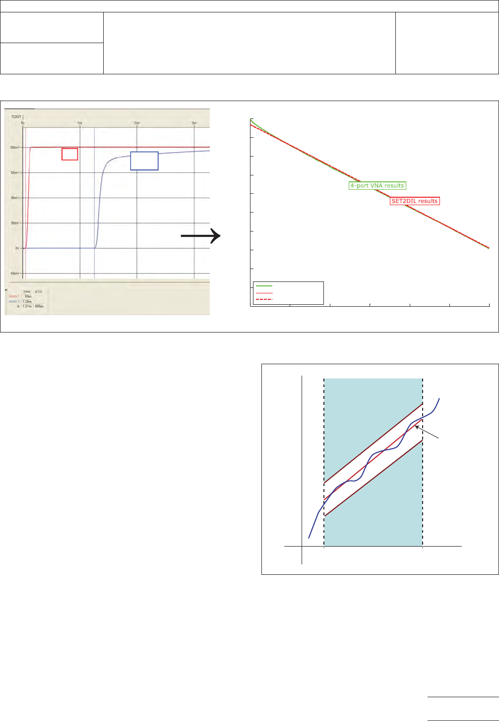
5.5.3 FD Measurement Adherence The metric used to
determine material ‘‘goodness’’ is insertion loss. Insertion loss
(IL) is defined as the negative of S21 expressed in decibels.
The through scattering parameter, S21, is a direct output from
the VNA or a TDT instrument. The insertion loss fit is used to
determine passing and failing lines. The slope the Insertion
loss fit, ma, can be used as another metric. Figure 5-20 illus-
trates the insertion loss of a line, the respective fit, and limit
regions.
The slope, m
a
, is representative of the average IL obtained
from the test sample. This slope should be less than the
slope, m
spec
, of the pass/fail line that is material dependent.
Figure 5-19 SET2DIL SDD21 Calculation
thru
SET2DIL
TDD21
0 2 4 6 8 10 12
x 10
9
-20
-18
-16
-14
-12
-10
-8
-6
-4
-2
0
VNA vs. SET2DIL (raw and fitted), L1, 100 ohms
Frequency (Hz)
SDD21 Magnitude (dB)
VNA 370HR
SET2DILraw 370HR
SET2DILfit 370HR
IPC-25512-5-20
Figure 5-20 Illustration of Insertion Loss Fit and Passing
and Failing Regions
Failing region high
Insertion
Loss
Fit Line
Failing region low
Frequencyf1
dB
f2
IPC-TM-650
Number
2.5.5.12
Subject
Test Methods to Determine the Amount of Signal Loss on
Printed Boards
Date
07/12
Revision
A
Page 23 of 24

5.5.4 Calculating Average Insertion Loss Slope m
a
and
Intercept b
a
For ‘‘N’’ points between frequency range f1to
f2 the average insertion loss slope and intercept are defined
as follows in Equations 5-15 to 5-18.
,
avg
=
1
N
Σ
n
,
n
[5-15]
IL
avg
=
1
N
Σ
n
IL(,
n
)
[5-16]
m
A
=
1
N
Σ
n
(,
n
− ,
avg
)⋅(IL(,
n
)−IL
avg
)
Σ
(,
n
− ,
avg
)
2
[5-17]
b
A
= IL
avg
− m
A
⋅ ,
avg
[5-18]
Suggested values of f1 and f2 are 1 GHz and 5 GHz respec-
tively.
The slope m
a
is a measure of the total frequency dependent
attenuation, α, which is described in IPC-2141.
IPC-TM-650
Number
2.5.5.12
Subject
Test Methods to Determine the Amount of Signal Loss on
Printed Boards
Date
07/12
Revision
A
Page 24 of 24
1 Scope This method describes the nondestructive mea-
surement of the relative permittivity and loss tangent of unclad
dielectric substrates at microwave frequencies using a split-
cylinder resonator (see Figure 1).
This test method is directly applicable for measuring the
in-plane (the plane parallel to the surface of the specimen)
permittivity of the specimen because the electric field is
in-plane. The permittivity of isotropic dielectrics can also be
measured with this method.
Note: This measurement method does not measure the out-
of-plane (direction normal to the surface of the specimen) per-
mittivity of the specimen. However, for most printed boards
the measurement uncertainties associated with this method
are typically less than the difference between in-plane and
out-of-plane permittivity values. Furthermore, comparison with
methods measuring the out-of-plane permittivity is difficult
because those methods typically do not provide measure-
ment confidence intervals.
2 Applicable Documents See 6.2.
3 Test Specimen The test specimen is an unclad dielectric
substrate. The substrate geometry can be either square or
circular as long as the substrate extends beyond the diameter
2a of the two cylindrical cavity sections as shown in Figure 2.
In particular, for the 10 GHz split-cylinder resonator discussed
in this method, the dimensions of the substrate should be at
least 50.0 mm [1.97 in] in diameter for circular samples or
50.0 mm [1.97 in] on a side for square samples.
Although the dielectric substrate thickness can vary from
0.05 mm to 5.0 mm [0.0020 in to 0.20 in], thin substrates may
lead to larger measurement uncertainties, while the dielectric
losses in thicker substrates may prevent the split-cylinder fix-
ture from resonating properly. A substrate thickness on the
order of 1.0 mm [0.040 in] is typical.
The measurement theory assumes the dielectric substrate has
a uniform thickness. Therefore, to reduce the measurement
uncertainty, variation and uncertainty in substrate thickness
should be minimized. A typical uncertainty in thickness should
be no more than 0.02 mm [0.00079 in]. In general, warped
samples should also be avoided as these can lead to biases
in the calculated values of the relative permittivity and loss
tangent.
For the split-cylinder resonator described here, the measure-
ment frequency of the split-cylinder resonator is a function of
the relative permittivity and thickness of the substrate. Thicker
substrates and higher values of relative permittivity drive the
resonant frequency lower, as shown in Figure 6.
IPC-25513-1
Figure 1 Split-Cylinder Resonator
IPC-25513-2
Figure 2 Split-Cylinder Resonator Diagram
Coupling
Loop
L
L
d
p
z
2a
2b
Coupling
Loop
Upper
Cylindrical
Cavity
Region
Lower
Cylindrical
Cavity
Region
Sample Region
3000 Lakeside Drive
Bannockburn, IL 60015-1249
IPC-TM-650
TEST METHODS MANUAL
Number
2.5.5.13
Subject
Relative Permittivity and Loss Tangent Using a
Split-Cylinder Resonator
Date
01/07
Revision
Originating Task Group
High Frequency Resonator Test Method Task Group
(D-24c)
Material in this Test Methods Manual was voluntarily established by Technical Committees of IPC. This material is advisory only
and its use or adaptation is entirely voluntary. IPC disclaims all liability of any kind as to the use, application, or adaptation of this
material. Users are also wholly responsible for protecting themselves against all claims or liabilities for patent infringement.
Equipment referenced is for the convenience of the user and does not imply endorsement by IPC.
Page1of4
ASSOCIATION CONNECTING
ELECTRONICS INDUSTRIES
®