IPC-TM-650 EN 2022 试验方法.pdf - 第673页
1 Scope This test method is used to characterize the cleanliness of printed wiring board fabrication processes by determining the degradation of electrical insulation resistance under conditions of high temperature and h…

5.3.3
One
uncoated specimen subjected to the same pro-
cessing (except coating) as the coated specimens shall be
supplied with each lot of samples as a test control.
5.4
Electrical Connections
5.4.1
Solder a single strand PTFE insulated wire, using the
flux specified in 4.9, to each pad of the D comb pattern.
These wires will be used to connect each pad of the desig-
nated comb pattern to polarization and insulation resistance
testing. When soldering the wires onto the pads care should
be taken to ensure that the flux does not splatter onto the
combs. A simple off-contact shield fixture should be used to
protect the test patterns from the flux spitting during solder-
ing.
Note: An alternate method is to use gold plated alligator clips.
5.5
Soldering Flux Removal
The
flux shall not be
removed. If the flux has contaminated the comb pattern on
the control, the sample shall be discarded and a new one
used. It cannot be cleaned because it will not represent the
cleaning process that was used prior to conformal coating
application.
5.6
Specimen Handling
For
the remainder of the test, the
surface of the test specimens either uncoated or coated with
conformal coating should not be handled or exposed to any
other contaminating influence.
5.7
Procedure
5.7.1
Condition
the specimens at 50 ± 2°C [122 ± 3.6°F]
with no added humidity, for a period of 24 hours.
5.7.2
Testing
5.7.2.1
Allow
the specimens to cool. Measure and record
the initial insulation resistance measurements at ambient labo-
ratory conditions. Apply 100 VDC on the specimen’s test
points with the resistance meter and take the reading after
one minute. On the D comb pattern, test points 1, 3 and 5 are
connected to the positive terminal and test points 2 and 4 are
connected to the negative terminal of the resistance meter.
5.7.2.2
Place
specimens in a chamber, in the vertical posi-
tion and under a condensation drip shield. Each chamber load
shall contain at least one uncoated board that is representa-
tive of the cleaning process used prior to conformal coating
application for each lot tested.
5.7.2.3
Close
chambers door and apply a 50 VDC polariz-
ing bias to all test patterns. Electrical connections to speci-
mens shall be made so that electrical polarization voltage and
the test voltage of the same polarity are connected to the
same terminal.
5.7.2.4 Expose
test specimens to 20 cycles of temperature
and humidity. Polarizing voltage shall be maintained through-
out the entire 20-cycle period. Humidity shall be maintained at
85% minimum through the cycles except that when going to
low temperature in Step c below, the humidity may drop to
80% minimum.
One cycle is as follows:
a. Start test at 25°C [77°F] and raise the temperature to 65°C
[149°F] over a time span of 1.75 ± 0.75 hours.
b. Maintain temperature at 65°C [149°F] for 3, +0.5, -0 hours
c. Lower the temperature from 65°C [149°F] to 25°C [77°F]
over 1.75 ± 0.5 hours
Note: There shall be no delay between cycles.
5.7.3
Measurement/Evaluation
5.7.3.1
Disconnect
50 VDC polarizing voltage source before
taking the insulation resistance measurements. Insulation
resistance shall be read as specified in 5.7.2.1.
5.7.3.2 Measure
and record the resistance at the first,
fourth, seventh and tenth cycle, between the 2nd and 3rd
hour of the high phase of each cycle. These measurements
are to be conducted without opening the chamber.
5.7.3.3
Upon
completion of the 20 cycles, the test comb
patterns shall be maintained at 25° ± 2°C [77° ± 3.6°F] rela-
tive humidity of 50 ± 5% for 24 hours.
5.7.3.4
After
the 24-hour stabilization, the insulation resis-
tance shall be measurements as previously stated in section
5.7.2.1.
5.7.3.5
The
comb patterns will be examined for appearance
and dielectric withstanding voltage in accordance with IPC-
CC-830.
IPC-TM-650
Number
2.6.3.4
Subject
Moisture
and Insulation Resistance –
Conformal Coating
Date
07/03
Revision
A
P
age2of2
电子技术应用 www.ChinaAET.com
1
Scope
This
test method is used to characterize the
cleanliness of printed wiring board fabrication processes by
determining the degradation of electrical insulation resistance
under conditions of high temperature and humidity.
This test method examines the cleanliness of a test substrate
prior to solder mask application, after solder mask application,
and after any final metalization and/or surface finish operation
(e.g., HASL or OSP), and may be used to demonstrate the
cleanliness of internal layers of a mulitilayer board prior to
lamination.
2
Applicable Documents
GR-78-CORE
Telcordia
Technologies (Formerly Bellcore)
2.1
Master Drawings
Telcordia
Technologies Test Pattern (GR-78-CORE, Figures
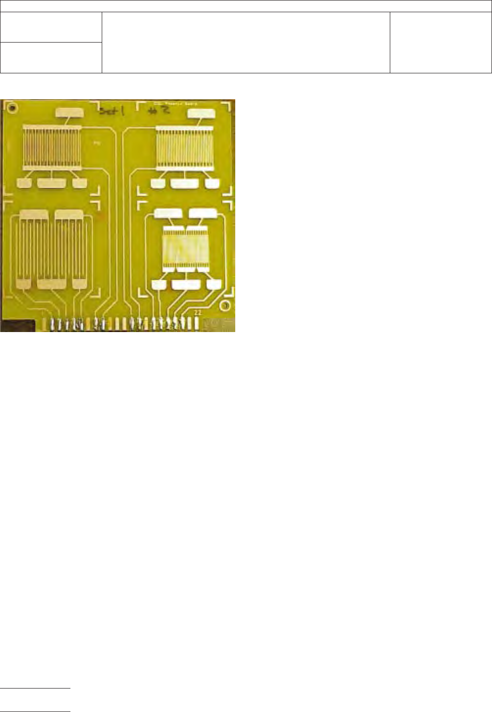
14.1 and 14.2)
IPC-B-50 Standard Test Board (Figure 3)
3
Test Specimens
The
test specimen for this test method
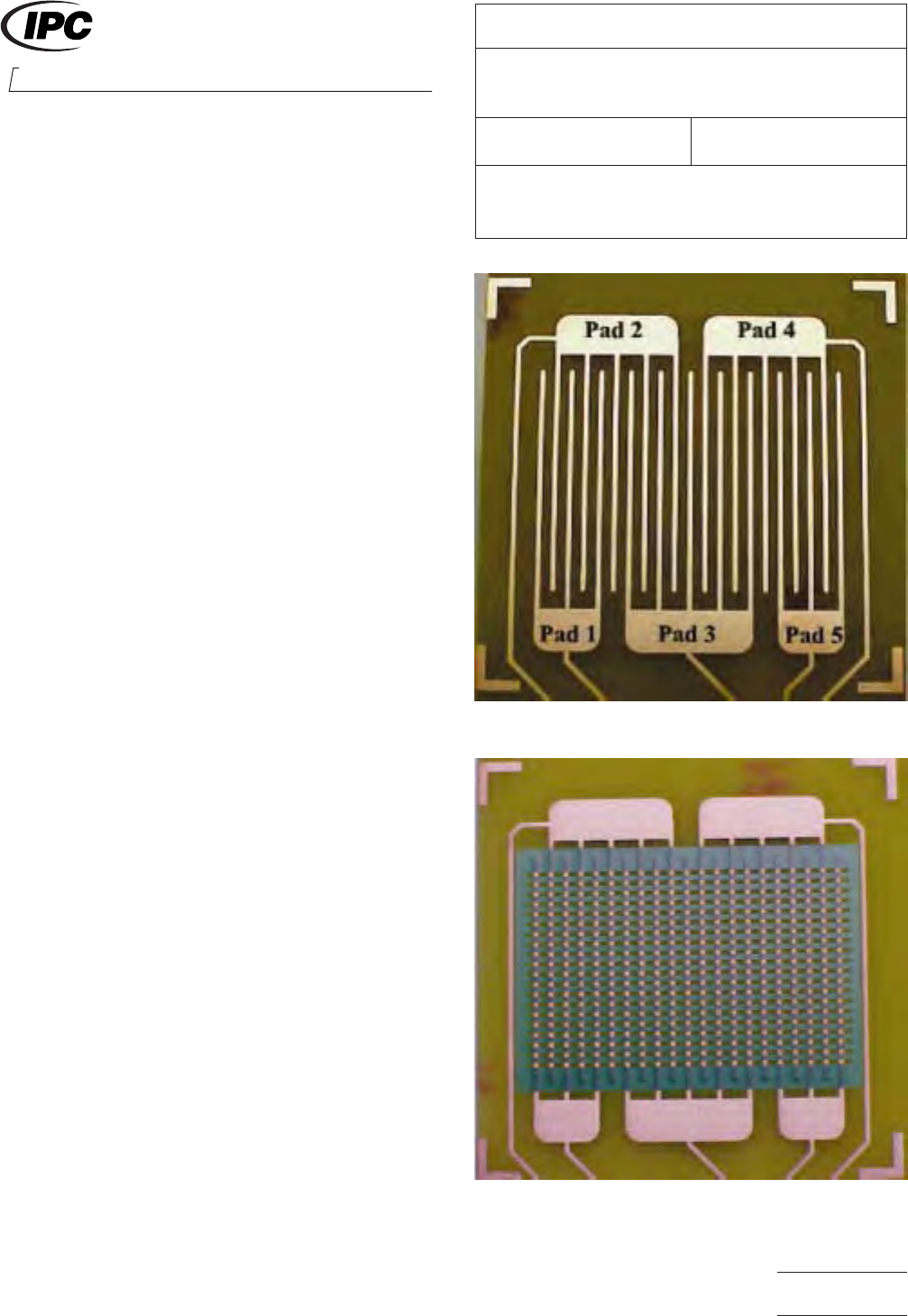
is the interdigitated comb pattern shown in Figures 1 and 2.
This test pattern can be produced in a number of formats, but
exists as one of the stock patterns of the IPC-B-50 standard
test board (see Figure 3).
This comb pattern has 0.65 mm [0.025 in] lines and 1.27 mm
[0.050 in] spacings. This test pattern is also commonly
referred to as the Bellcore pattern. When used for qualification
purposes, the base laminate will be FR-4 epoxy-glass with
17 µm [0.5 oz equivalent] unprotected copper metalization.
4
Apparatus
4.1
Clean
test chamber capable of producing and recording
an environment of 35°C ± 2°C [95°F ± 3.6°F] and 87.5% ±
2.5% relative humidity, and that allows the insulation resis-
tance of the patterns to be measured under these conditions.
The chamber must be capable of holding these conditions
under load (i.e., with samples in place).
Figure
1 Interdigitated Comb Pattern
Figure
2 With Solder Mask
2215
Sanders Road
Northbrook, IL 60062-6135
IPC-TM-650
TEST
METHODS MANUAL
Number
2.6.3.5
Subject
Bare
Board Cleanliness by Surface Insulation
Resistance
Date
01/04
Revision
Originating Task Group
Bare Board Cleanliness Assessment Task Group
(5-32c)
Material
in this Test Methods Manual was voluntarily established by Technical Committees of IPC. This material is advisory only
and its use or adaptation is entirely voluntary. IPC disclaims all liability of any kind as to the use, application, or adaptation of this
material. Users are also wholly responsible for protecting themselves against all claims or liabilities for patent infringement.
Equipment referenced is for the convenience of the user and does not imply endorsement by IPC.
P
age1of4
ASSOCIA
TION CONNECTING
ELECTRONICS INDUSTRIES
®
电子技术应用 www.ChinaAET.com
4.2
A
resistance meter capable of reading high resistance
(10
12
ohms)
with a test voltage of 100 ± 2 volts DC or an
ammeter capable of reading 10
-10
amperes
in combination
with 100 volts DC power supply. Standard resistors should be
used for routine calibration.
5
Test
5.1 Sample Sizes
•
Eight test patterns are produced for test with no applied
solder mask (Figure 1).
• Eight test patterns are produced for test with solder mask
applied, imaged, and cleaned (Figure 2).
• Eight test patterns are produced for test with solder mask
applied and the final finish in place (e.g., HASL).
5.2
Specimen Identification
Use
a noncontaminating
method for identifying the test specimen (e.g., vibrating
scribe). During this process, handle the specimens by the
edges only or using noncontaminating gloves.
5.3
Wire Attach
Cover
the test patterns with noncontami-
nating barrier, such as aluminum foil or plastic film, to prevent
flux spattering during the wire attach process. Use water
white rosin to solder PTFE-insulated wires to the connection
points of the specimens. Do not attempt to remove the flux
residues. Alternatively, connections may be made by
mechanical pressure connections (e.g., alligator clips).
NOTE: Because of the very high resistance levels typically
used as pass-fail criteria for this method, a connector-based
or other fixtured setup is not recommended, due to leakage
currents, unless these systems can be shown to have no sig-
nal degradation compared to hardwiring.
5.4
Placing in Chamber
Place
the specimens in the envi-
ronmental chamber in a vertical position such that the airflow
is parallel to the direction of the board in the chamber. Allow
at least 2.5 cm [0.98 in] between each test sample. Dress all
wiring away from the test patterns. Route the wires to the
outside of the chamber. Set the chamber temperature to
35°C [95°F] and 85% minimum relative humidity, with a ramp
time of not less than one hour. There is no electrical potential
applied to any test pattern during the first 24 hours of test
exposure.
5.5
Resistance Measurements
After
24 hours of test
exposure with no applied electrical potential, measure the
insulation resistance of each pattern using an applied voltage
of 100 ± 2 volts DC and an electrification time of 60 seconds.
NOTE: It is recommended that the temperature and humidity
levels be verified to be within the recommended limits prior to
beginning the resistance measurements.
Each comb pattern represents four test measurements. Mea-
surements are made between (see Figure 1):
• Pad 1 to Pad 2
• Pad 3 to Pad 2
• Pad 3 to Pad 4
• Pad 5 to Pad 4
Pads 2 and 4 are at one potential and Pads 1, 3, and 5 are at
the opposite potential (see Note 6.3).
All measurements are to be taken with the specimens at the
test conditions and inside the chamber (in-situ).
Determine the means of the dataset as outlined in 5.6.
If, after 24 hours, the results conform to the specification,
record the values and terminate the test.
If, after 24 hours, the results do not conform to the specifica-
tion, then the test may be extended to 96 hours of exposure
to the test conditions with no applied electrical potential.
Figure
3 IPC-B-50
IPC-TM-650
Number
2.6.3.5
Subject
Bare
Board Cleanliness by Surface Insulation Resistance
Date
01/04
Revision
P
age2of4
电子技术应用 www.ChinaAET.com